Inspection unit

a technology of inspection unit and plunger, which is applied in the direction of coupling device connection, semiconductor/solid-state device testing/measurement, instruments, etc., can solve the problems of inability to achieve smooth movement of the plunger to be achieved by the spring within the pipe, impedance or other measurement factors fluctuation, etc., to achieve high reliability and inspection. high, not so expensive, easy to manufacture

Active Publication Date: 2006-10-24
YOKOWO CO LTD
View PDF5 Cites 17 Cited by
  • Summary
  • Abstract
  • Description
  • Claims
  • Application Information

AI Technical Summary

Benefits of technology

[0012]It is therefore an object of the invention to provide an inspection unit which can perform highly reliable inspection without being affected by noises, employing contact probes of a coaxial structure which can be easily manufactured but are not so expensive, even in a case where an inspection is conducted with respect to a device for RF signals in which electrode terminals are arranged with a very narrow pitch as small as 0.4 mm.

Problems solved by technology

On occasion of inspecting electrical performance of the RF device such as a semi-conductor wafer, an IC, or a module, insufficient contacts between the terminals may particularly cause fluctuation of impedance or other measurement factors, which may sometimes vary to change measured values.
In this respect, there has been a problem that the contact probe is liable to be crooked with an external force, and even with a little crook, smooth movement of the plunger to be achieved by the spring within the pipe may be hindered.
Moreover, in a case where the dielectric ring is made larger in width with a view to enhancing easiness in its insertion process and mechanical strength, the dielectric constant of the dielectric substance in the coaxial structure becomes larger, resulting in disturbance of the characteristic impedance, which will sacrifice the high frequency characteristics and high speed performance.
However, this structure has also a problem that when the metal plate 31 is mounted after the contact probes 1 have been inserted, the contact probes 1 in the coaxial structure may be inclined, as shown in FIG. 8B, and a work for mounting the metal plate 31 is difficult because several hundreds of the contact probes including the contact probes for power supply and grounding are present within an area of a few cm2, and each the contact probe in the coaxial structure has a diameter of about 0.15 mm and a length of a few millimeter.

Method used


Image

  • Inspection unit
  • Inspection unit
  • Inspection unit

Examples


Embodiment Construction

[0037]Embodiments of the invention will be described with reference to the accompanying drawings.

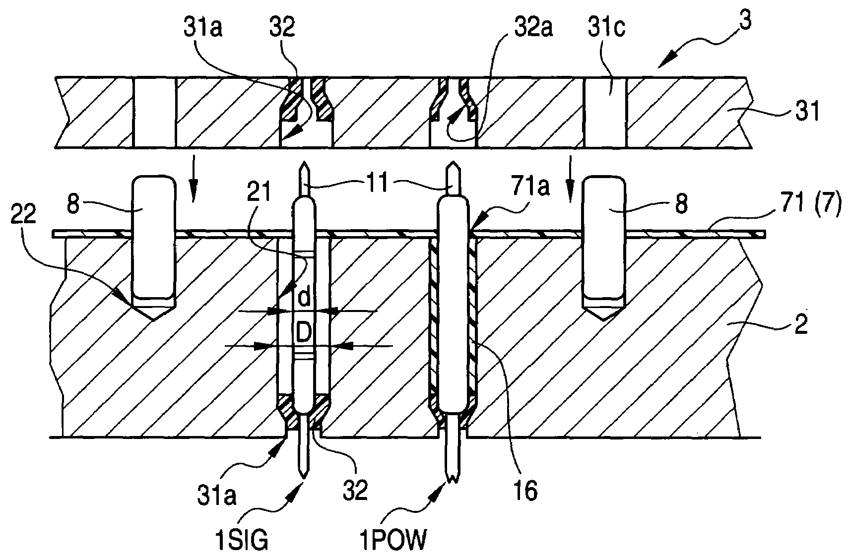
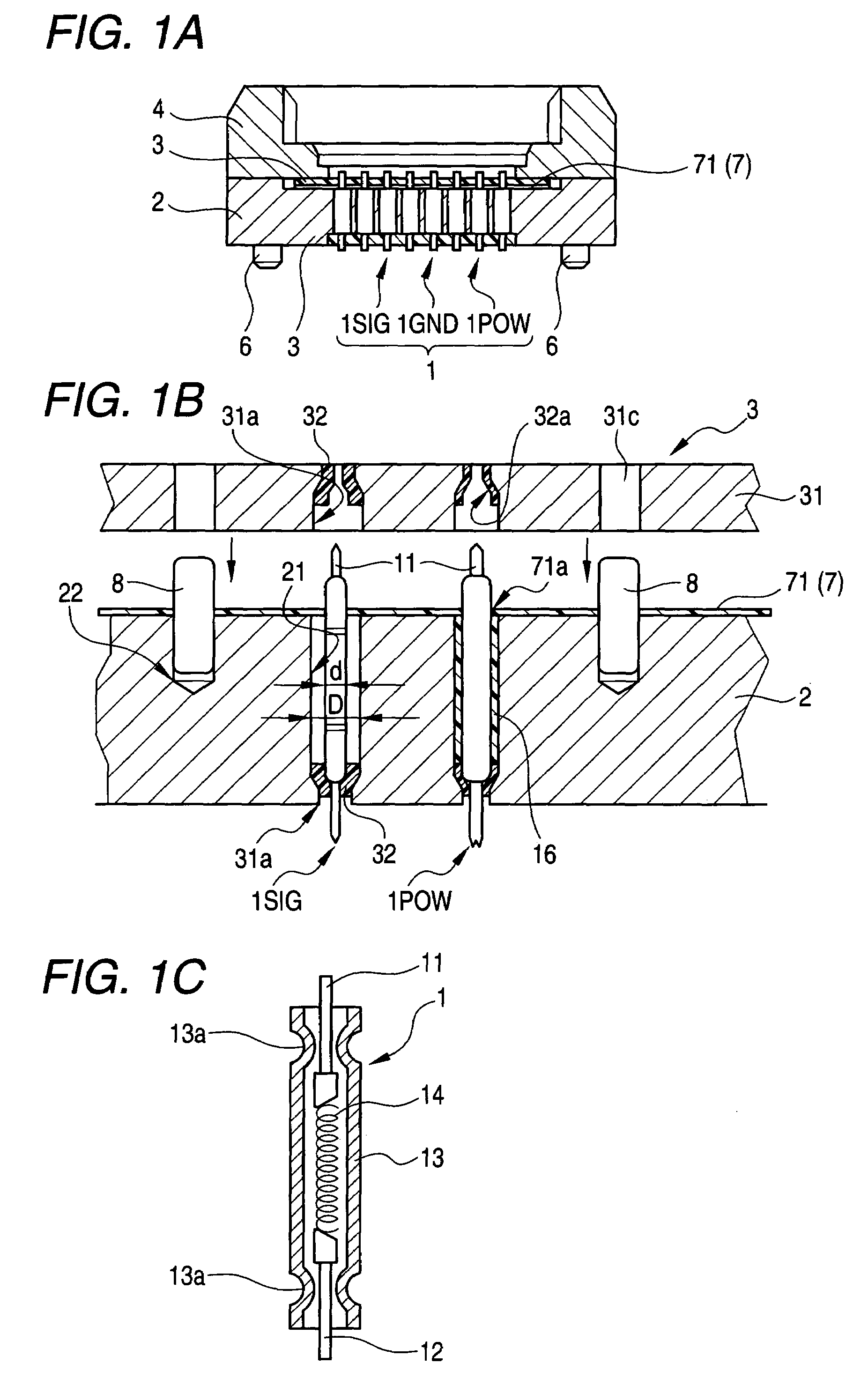
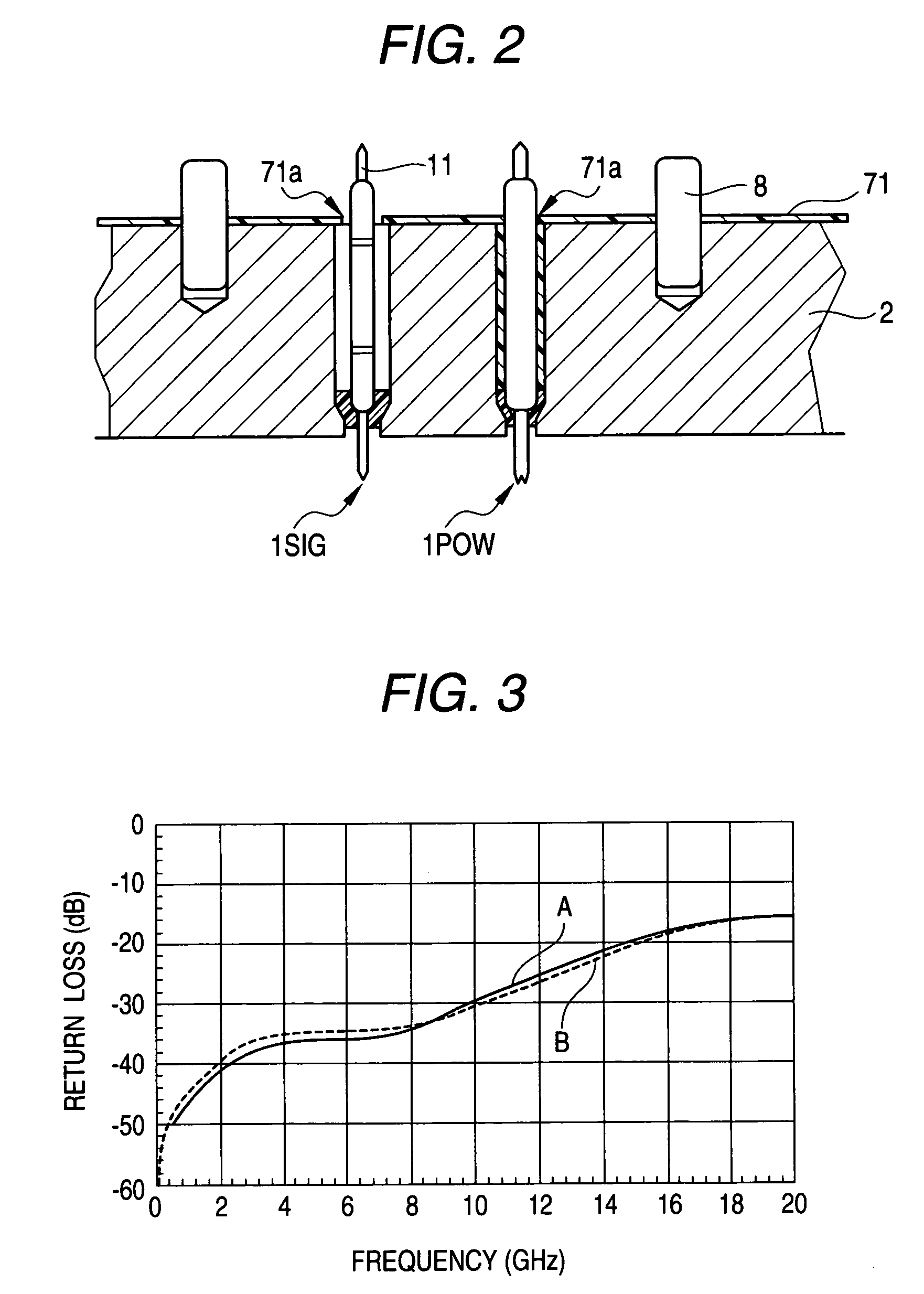
[0038]As shown in FIG. 1, an IC socket according to a first embodiment of the invention comprises a metal block 2 formed with through holes 21. Within one of the through holes 21, a contact probe 1SIG for RF signals is disposed while leaving a gap, so as to be a core conductor of a coaxial structure, and further, contact probes 1POW, 1GND for power supply and for grounding are respectively provided in other through holes 21 of the metal block 2. A first retainer 3 for fixing the contact probes 1SIG, 1POW, 1GND so as not to escape from the metal block 2, while only plungers 11 of the contact probes 1SIG, 1POW, 1GND are projected, is provided on one face of the metal block 2. There is further provided a second retainer 7 for holding tip ends of the contact probes 1SIG, 1POW, 1GND at positions to be opposed to through holes 31a for the plungers 11 formed in the first retainer 3.

[0039]In thi...


PUM


Abstract

A conductive member has a first face adapted to be mounted on a board on which an inspection circuit is arranged and a second face adapted to be opposed to a device to be inspected. The conductive member being formed with a first through hole having a first diameter and communicating the first face with the second face. A contact probe is provided with a tubular body having a second diameter which is smaller than the first diameter, and a plunger retractably projected from one end of the tubular body. A first retainer is formed with a second through hole and opposing at least the second face of the conductive member so as to communicate the first through hole with the second through hole, so that the contact probe is retained in the conductive member while only the plunger is projected from one end of the second through hole. A second retainer is adapted to retain the one end of the tubular body concentrically with the first through hole.

Description

BACKGROUND OF THE INVENTION[0001]The present invention relates to an inspection unit for a high frequency / high-speed device for ensuring reliable connection between the inspection unit and the device to be inspected, on occasion of inspecting its electrical performance, before a module of a high frequency / high-speed circuit such as an amplifier circuit, a mixer circuit, a filter circuit, a memory, a CPU, etc. or an IC to be incorporated in a mobile phone, for example, has been assembled to a circuit board. In this specification, the term “high frequency” refers to an analogue signal having a high frequency (1 GHz or more), while the term “high-speed” refers to a digital signal having very short pulse width and pulse interval, and both of which are hereinafter collectively referred to as RF (radio frequency).[0002]On occasion of inspecting electrical performance of the RF device such as a semi-conductor wafer, an IC, or a module, insufficient contacts between the terminals may partic...

Claims


Application Information

Patent Timeline
Patent Type & Authority Patents(United States)
IPC IPC(8): G01R31/02G01R1/06G01R1/067G01R1/073G01R31/26H01R13/646H01R13/658H01R13/6588H01R24/40H01R33/76
CPCG01R1/06772G01R1/07314G01R1/07371G01R1/07378G01R1/06722G01R1/067G01R31/26H01L22/00
Inventor YOSHIDA, TAKUTOSATO, ATSUSHI
Owner YOKOWO CO LTD
Why Eureka
Try Eureka