Method and system for calibrating a light emitting device display

a technology of light-emitting devices and display devices, applied in the field of light-emitting device display, can solve the problems of low mobility and device instability, low-cost manufacturing of poly-silicon backplanes, and the lik

Active Publication Date: 2006-07-06
IGNIS INNOVATION
View PDF9 Cites 145 Cited by
  • Summary
  • Abstract
  • Description
  • Claims
  • Application Information

AI Technical Summary

Benefits of technology

[0010] It is an object of the invention to provide a method and system that obviates or mitigates at least one of the disadvantages of existing systems.

Problems solved by technology

However, due to its relative infancy, ongoing processing concerns, and limited available capacity, the usage of the poly-silicon backplanes does not lend itself to low-cost manufacturing.
However the usage of a-Si in AMOLED backplanes encounters two issues, namely low mobility and device instability due to the shift of the threshold voltage of a transistor.
[Ref. 1] may face a “settling time” problem due to the low transconductance of the a-Si TFT coupled with a high line capacitance.
However, they require techniques to decrease the dependence of OLED current on the threshold shift of a thin film transistor (TFT).
However they either use complex pixel circuits, each having more than 2 TFTs and / or have programming methods which suffer from the same programming time issues as with current programmed circuits.

Method used


Image

  • Method and system for calibrating a light emitting device display
  • Method and system for calibrating a light emitting device display
  • Method and system for calibrating a light emitting device display

Examples


Embodiment Construction

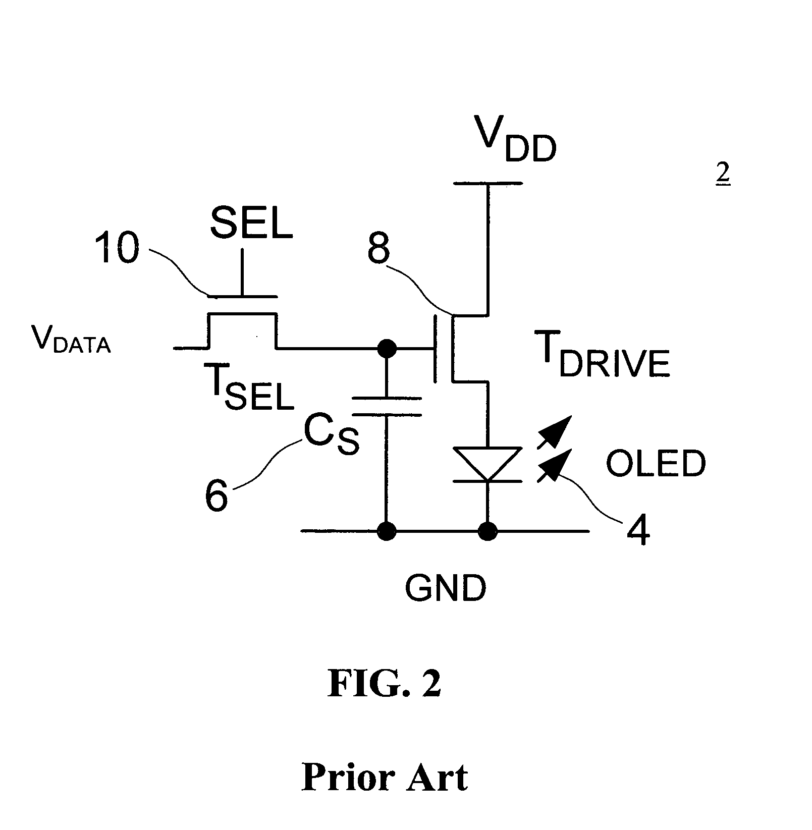
[0020] Embodiments of the present invention is described using a pixel circuit having an organic light emitting diode (OLED) and a drive thin film transistor (TFT). However, the pixel circuit described herein may include a light emitting device other than the OLED, and may include a transistor(s) other than the TFT. It is noted that in the description, “pixel circuit” and “pixel” may be used interchangeably.

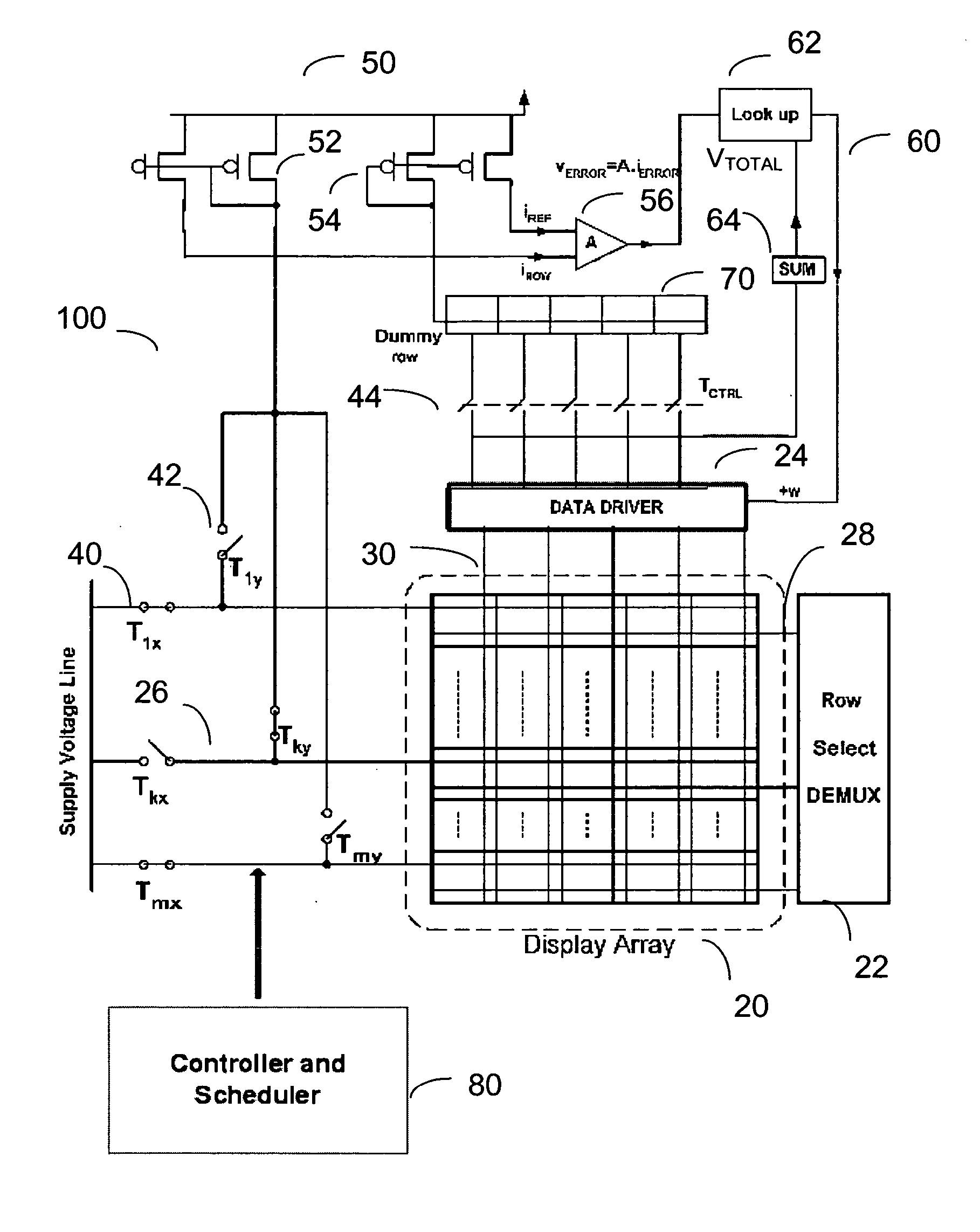
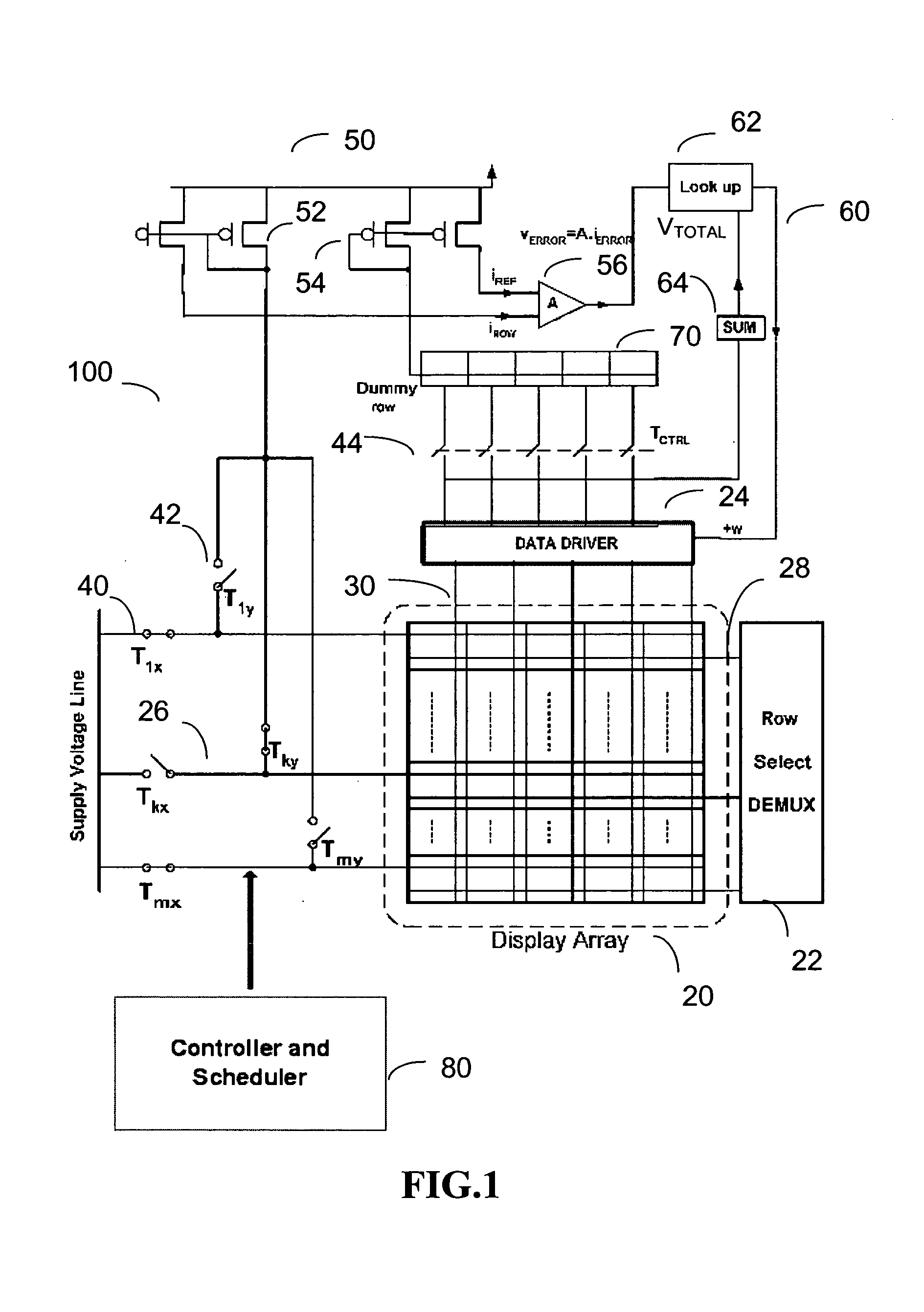
[0021]FIG. 1 is a diagram showing system architecture for implementing a calibration technique in accordance with an embodiment of the present invention to a display array 20. Referring to FIG. 1, an external calibration system 100 is provided outside the display array 20. The calibration system 100 includes a switch network system for selectively implementing one of a normal display operation and a calibration operation to the display array 20, an error extraction system 50 for extracting error information related to the shift of the characteristic(s) of a pixel using a dummy r...


PUM


Abstract

A method and system for calibrating a light emitting device display is provided. The display includes a plurality of pixel circuits, each having a light emitting device. The system for the calibration monitors current drawn from a row of the display array, and generates a correction parameter to correct brightness level of the light emitting device.

Description

FIELD OF INVENTION [0001] The present invention relates to a light emitting device display, and more specifically to a method and system for calibrating the light emitting device display. BACKGROUND OF THE INVENTION [0002] Recently active-matrix organic light-emitting diode (AMOLED) displays with amorphous silicon (a-Si), poly-silicon, organic, or other driving backplane have become more attractive due to advantages over active matrix liquid crystal displays (AMLCDs). For example, the advantages include: lower power, wider viewing angle, and faster refresh rate displays. [0003] Currently most of the AMOLED displays use poly-silicon backplanes. However, due to its relative infancy, ongoing processing concerns, and limited available capacity, the usage of the poly-silicon backplanes does not lend itself to low-cost manufacturing. [0004] By contrast, amorphous silicon (a-Si) leverages the vast installed infrastructure of proven AMLCD production, promising much lower manufacturing costs...

Claims


Application Information

Patent Timeline
Patent Type & Authority Applications(United States)
IPC IPC(8): G06F19/00G09G3/3225
CPCG09G3/3233G09G3/3291G09G2300/0417G09G2300/0842G09G2320/0233G09G2320/029G09G2320/0693
Inventor SAMBANDAN, SANJIVSERVATI, PEYMANNATHAN, AROKIA
Owner IGNIS INNOVATION
Why Eureka
Try Eureka