Integrated circuit yield enhancement using voronoi diagrams

a voronoi diagram and integrated circuit technology, applied in error detection/correction, instruments, program control, etc., can solve problems such as random defects, adversely affecting yield, and yield loss, so as to reduce critical area contribution cost, and optimize the position and length of edges

Inactive Publication Date: 2006-07-06
GLOBALFOUNDRIES INC
View PDF8 Cites 23 Cited by
  • Summary
  • Abstract
  • Description
  • Claims
  • Application Information

AI Technical Summary

Benefits of technology

[0013] The invention provides a method of calculating critical area in an integrated circuit design. Starting with an initial integrated circuit design, the invention associates variables with the positions of the edges in the design. The invention associates cost functions involving the variables with the spacing among (between) these edges. The cost functions are in terms of critical area contributions. Critical area contributions comprise a

Problems solved by technology

While this capability grants performance, the smaller size and higher density of layout features adversely affect yield [See: Papadopoulou, E., “Critical area computation for missing material defects in VLSI circuits, “Computer-Aided Design of Integrated Circuits and Systems, IEEE Transactions on, Vol. 20, No. 5, pp 583-597, May 2001; Fook-Luen Heng and Zhan Chen.
Both the manufacturing process and geom

Method used


Image

  • Integrated circuit yield enhancement using voronoi diagrams
  • Integrated circuit yield enhancement using voronoi diagrams
  • Integrated circuit yield enhancement using voronoi diagrams

Examples


Embodiment Construction

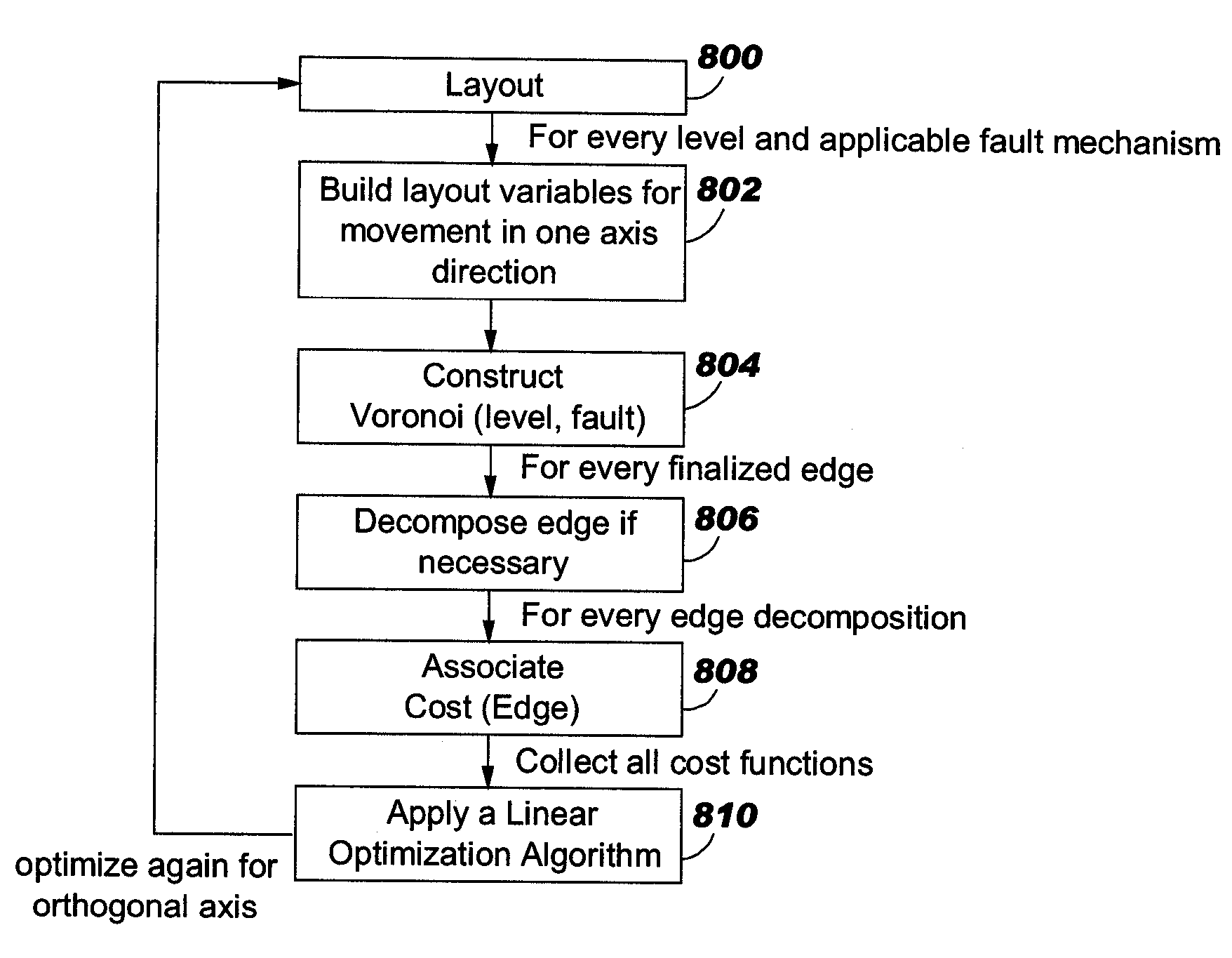
[0053] The present invention and the various features and advantageous details thereof are explained more fully with reference to the non-limiting embodiments that are illustrated in the accompanying drawings and detailed in the following description. It should be noted that the features illustrated in the drawings are not necessarily drawn to scale. Descriptions of well-known components and processing techniques are omitted so as to not unnecessarily obscure the present invention. The examples used herein are intended merely to facilitate an understanding of ways in which the invention may be practiced and to further enable those of skill in the art to practice the invention. Accordingly, the examples should not be construed as limiting the scope of the invention.

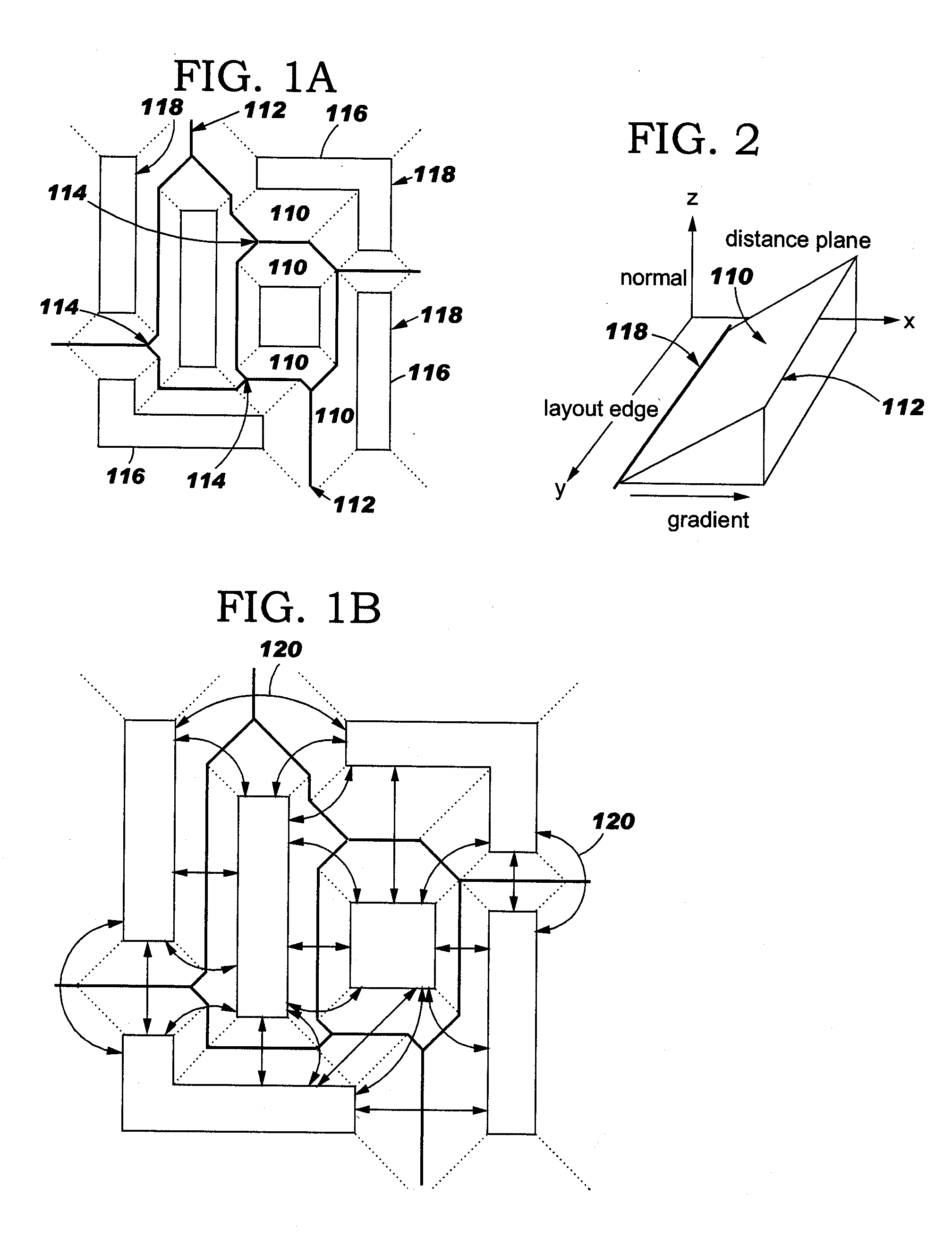
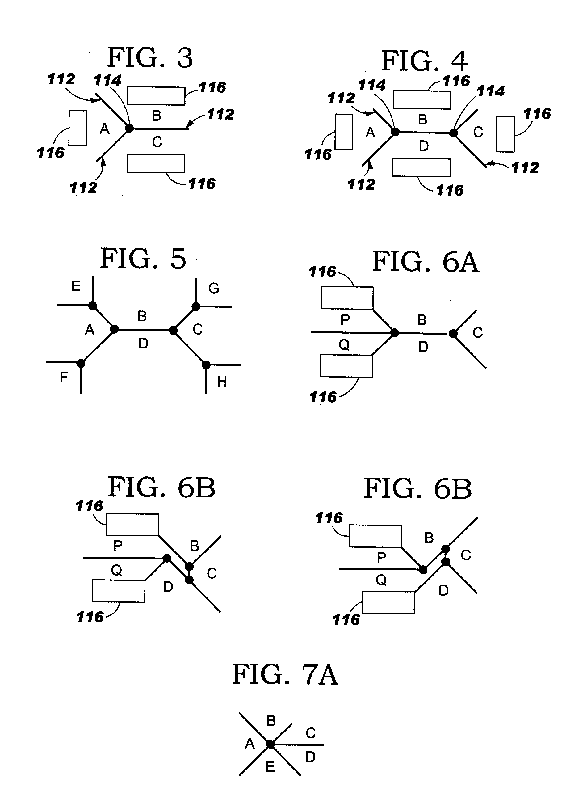
[0054] First, the invention constructs a weighted Voronoi diagram (shown in FIGS. 1A and 1B) for a particular electrical fault mechanism using known techniques. Denote this as Voronoi (fault). Electrical fault mechanisms ...


PUM


Abstract

A method of calculating critical area in an integrated circuit design, said method comprising: inputting an integrated circuit design; associating variables with the positions of edges in said integrated circuit design; and associating cost functions of said variables with spacing between said edges in said integrated circuit design; wherein said cost functions calculate critical area contributions as the positions and length of said edges in said integrated circuit design change, and wherein said critical area contributions comprise a measure of electrical fault characteristics of said spacing between said edges in said integrated circuit design.

Description

CROSS REFERENCE TO RELATED APPLICATIONS [0001] The present application is related to pending U.S. patent application Ser. No. 10 / ______, filed concurrently herewith to Allen et al., entitled “CRITICAL AREA COMPOSITE FAULT MECHANISMS USING VORONOI DIAGRAMS” (IBM Docket No. BUR920030136US1). The foregoing application is assigned to the present assignee, and is incorporated herein by reference.BACKGROUND OF INVENTION [0002] 1. Field of the Invention [0003] The present invention generally relates to measuring critical area in integrated circuit design, and more particularly to a method that uses Voronoi diagrams to measure critical area as the design layout is changed. [0004] 2. Description of the Related Art [0005] Within this application several publications are referenced by Arabic numerals within parentheses. Full citations for these, and other, publications may be found at the end of the specification immediately preceding the claims. The disclosures of all these publications in th...

Claims


Application Information

Patent Timeline
IPC IPC(8): G06F17/50G06F9/45
CPCG06F17/5081G06F30/398
Inventor ALLEN, ROBERT J.GRAY, MICHAEL S.HIBBELER, JASON D.TAN, MERVYN YEE-MINWALKER, ROBERT F.
Owner GLOBALFOUNDRIES INC
Why Eureka
Try Eureka