On-chip self test circuit and self test method for signal distortion

a self-testing and signal technology, applied in the field of test circuits, can solve the problems of expensive equipment having a small self-load, a lot of time and physical cost for window measurement of output signals,

Active Publication Date: 2006-07-13
SK HYNIX INC
View PDF12 Cites 36 Cited by
  • Summary
  • Abstract
  • Description
  • Claims
  • Application Information

AI Technical Summary

Problems solved by technology

Since a window of an output signal in a conventional memory device is measured by simply connecting an output pad to an external test device, the window measurement of the output signal r...

Method used


Image

  • On-chip self test circuit and self test method for signal distortion
  • On-chip self test circuit and self test method for signal distortion
  • On-chip self test circuit and self test method for signal distortion

Examples


Embodiment Construction

[0023] Hereinafter, the preferred embodiments of the present invention will be described in detail referring to the accompanying drawings.

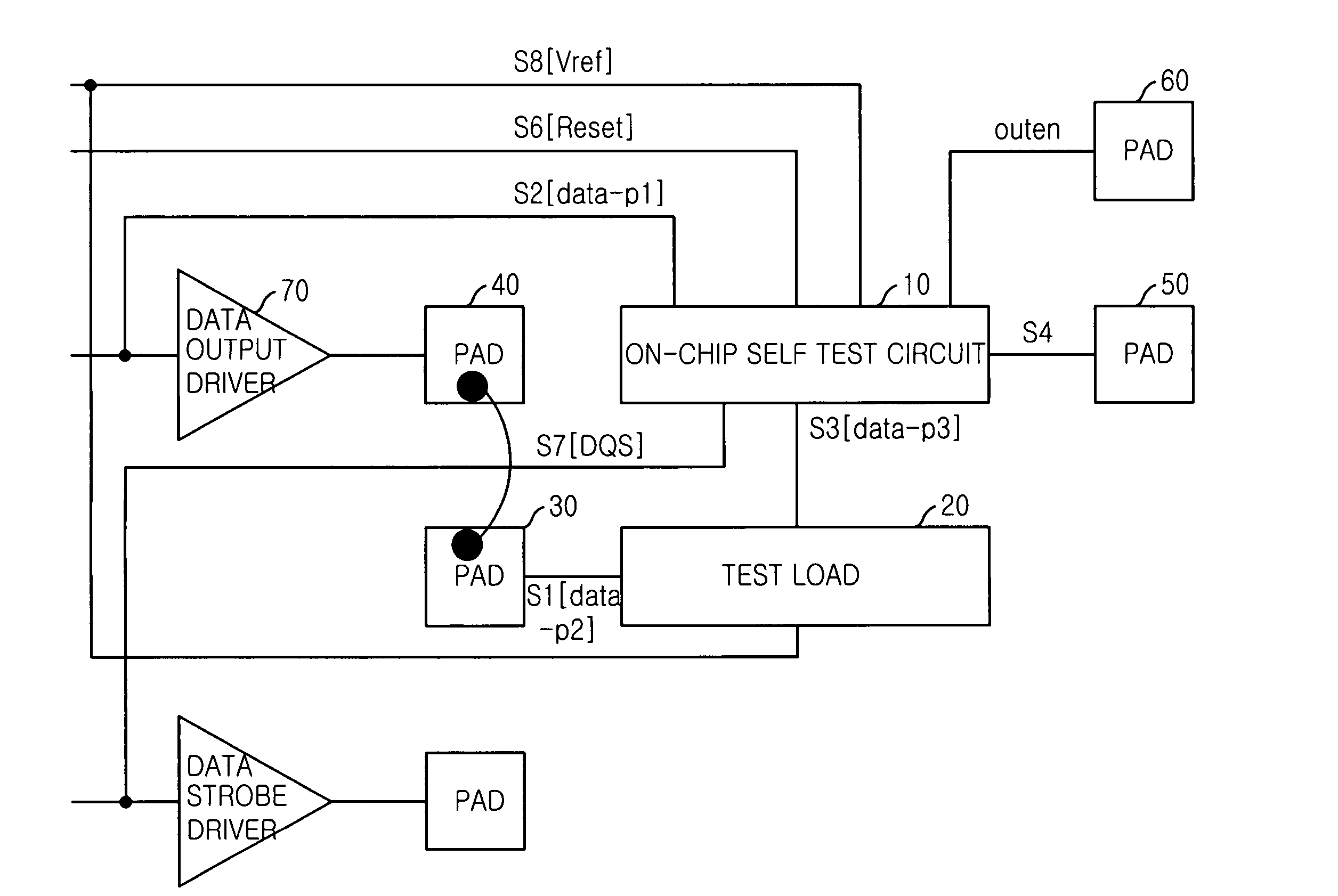
[0024] The present invention provides an on-chip self test circuit having a self test block and a test load on a target chip. Accordingly, the one-chip self test circuit can measure window of data output signal so as to measure a validity of an enable window of specific signal or synchronization validity.

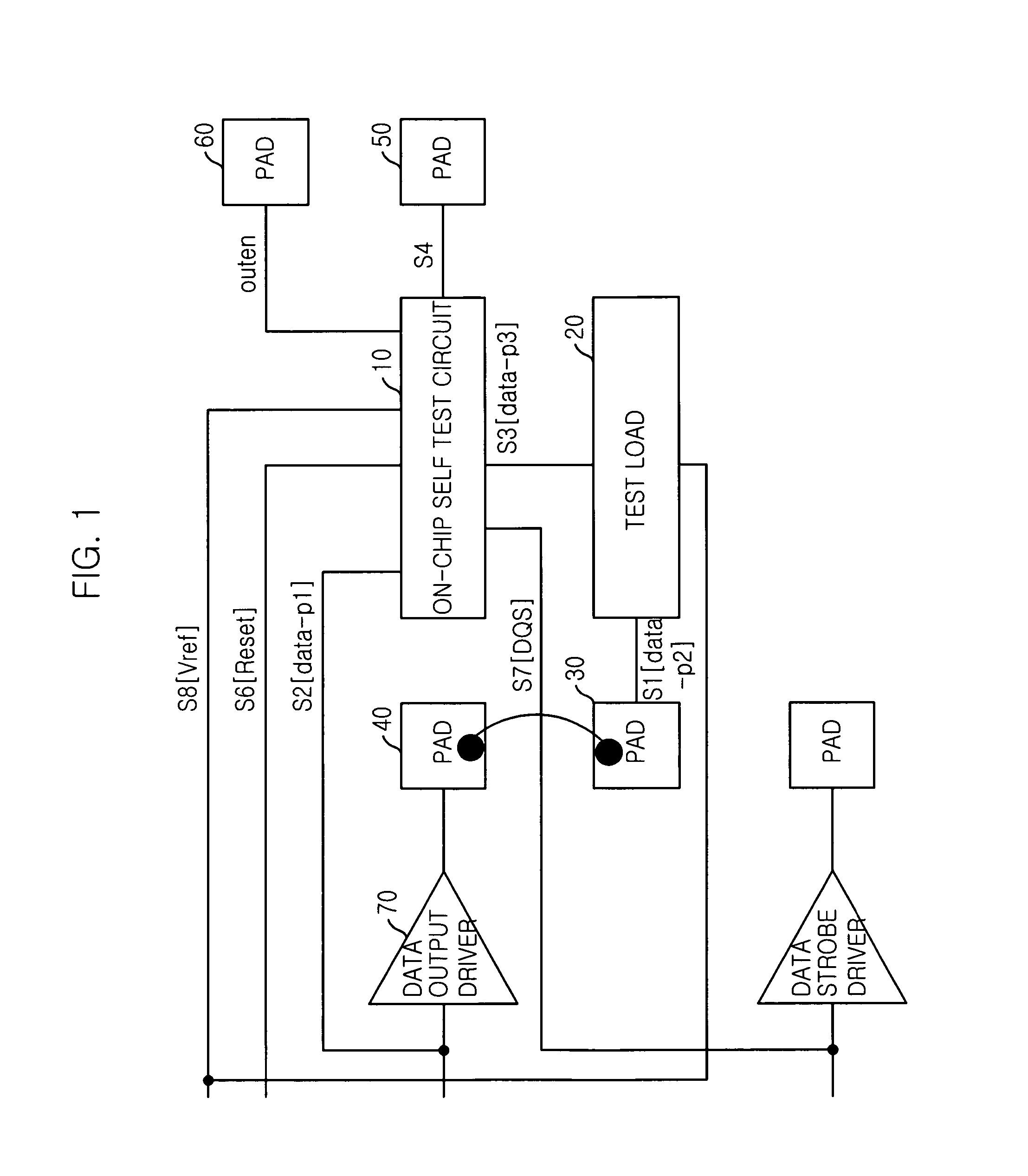
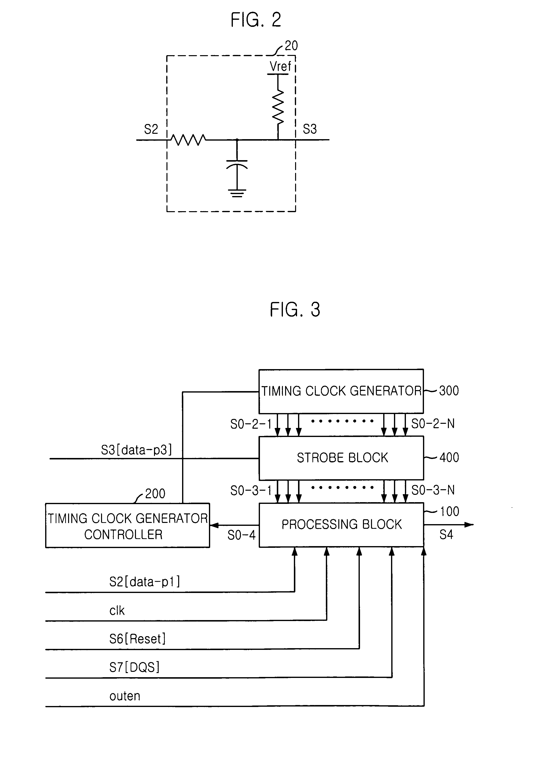
[0025]FIG. 1 is a block diagram of an on-chip self test circuit in accordance with an embodiment of the present invention. In FIG. 1, a self test block 10 is a circuit block that measures a window validity of a test target signal, and a test load block 20 is a block that is implemented inside a chip so as to provide a circuit component similar to a case where it is connected to an external chip.

[0026] In this embodiment, an on-chip self test circuit may further include a selecting unit for selecting a test target signal among several signals ou...


PUM


Abstract

There is provided an on-chip test circuit that is capable of measuring validity of an output signal within a chip without any external measuring device. The on-chip self test circuit implemented on the same chip as a test semiconductor device includes: a test load block for receiving a test target signal; and a self test block for receiving a test target signal passing through the test load block and a test target signal inputted to an output driver together, and determining whether a change of the test target signal is within an allowable range. Accordingly, the validity of the signal outputted from the device can be measured without any expensive external measuring device. Also, when the test must be done before the packaging stage, the test can be simply performed, thereby reducing the test cost greatly.

Description

FIELD OF INVENTION [0001] The present invention relates to a test circuit implemented on a chip; and, more particularly, to an on-chip test circuit that is capable of measuring a window of a signal without any connection to an external measuring device. DESCRIPTION OF PRIOR ART [0002] A general method for guaranteeing a correct operation of a memory device is to measure a window of output signals. The window is an important factor for synchronizing an external device with data input / output. [0003] Since a window of an output signal in a conventional memory device is measured by simply connecting an output pad to an external test device, the window measurement of the output signal requires a lot of time and a lot of manpower / physical cost. Specifically, when an unpackaged chip is sold, the window measurement is performed in a wafer level. However, in order to monitor a radio frequency (RF) output in the wafer level, expensive equipment having a small self-load is required. SUMMARY OF...

Claims


Application Information

Patent Timeline
IPC IPC(8): G01R31/02
CPCG01R31/31708G01R31/3187G11C29/02G11C29/023G11C29/028G11C29/12015G11C29/40G11C29/50G11C29/50012G01R31/31713G01R31/3177
Inventor KIM, KYUNG-HOON
Owner SK HYNIX INC
Why Eureka
Try Eureka