Semiconductor integrated circuit, layout method, layout apparatus and layout program

Active Publication Date: 2006-07-20
RENESAS ELECTRONICS CORP
View PDF25 Cites 8 Cited by
  • Summary
  • Abstract
  • Description
  • Claims
  • Application Information

AI Technical Summary

Benefits of technology

[0013] Accordingly, an object of the present invention is to provide a semiconductor integrated circuit, layout method, layout apparatus and layout program that make it possible to suppress a decline in wiring ability.
[0018] In accordance with the present invention, it is possible to minimize the wiring tracks superposed by the wiring of the first and second wiring layers and by the via units, and effective wiring resources (the number of wiring tracks) can be increased (wiring ability can be improved). Further, since implementation is possible without reducing the number of vias, the invention can be implemented without diminishing resistance to EM.
[0019] Further, in accordance with the present invention, layout convergence can be improved (TAT is shortened), an increase in chip size can be suppressed and cost can be reduced.

Problems solved by technology

As a result of strengthening the power wiring structure within a semiconductor integrated circuit according to the prior art, a problem which arises is a reduction in wiring resources (number of tracks) effects as wiring traces within the semiconductor integrated circuit.
However, since there is the danger that wiring ability cannot be improved, a problem which arises is an increase in chip size.
Further, the following problems arise with the structural examples illustrated in FIGS.
This reduces the effective wiring resources.
In addition, processing of the wiring formed in the areas of the VDD wiring of M1 and GND wiring of M1 is difficult and cell size increases.

Method used


Image

  • Semiconductor integrated circuit, layout method, layout apparatus and layout program
  • Semiconductor integrated circuit, layout method, layout apparatus and layout program
  • Semiconductor integrated circuit, layout method, layout apparatus and layout program

Examples


first embodiment

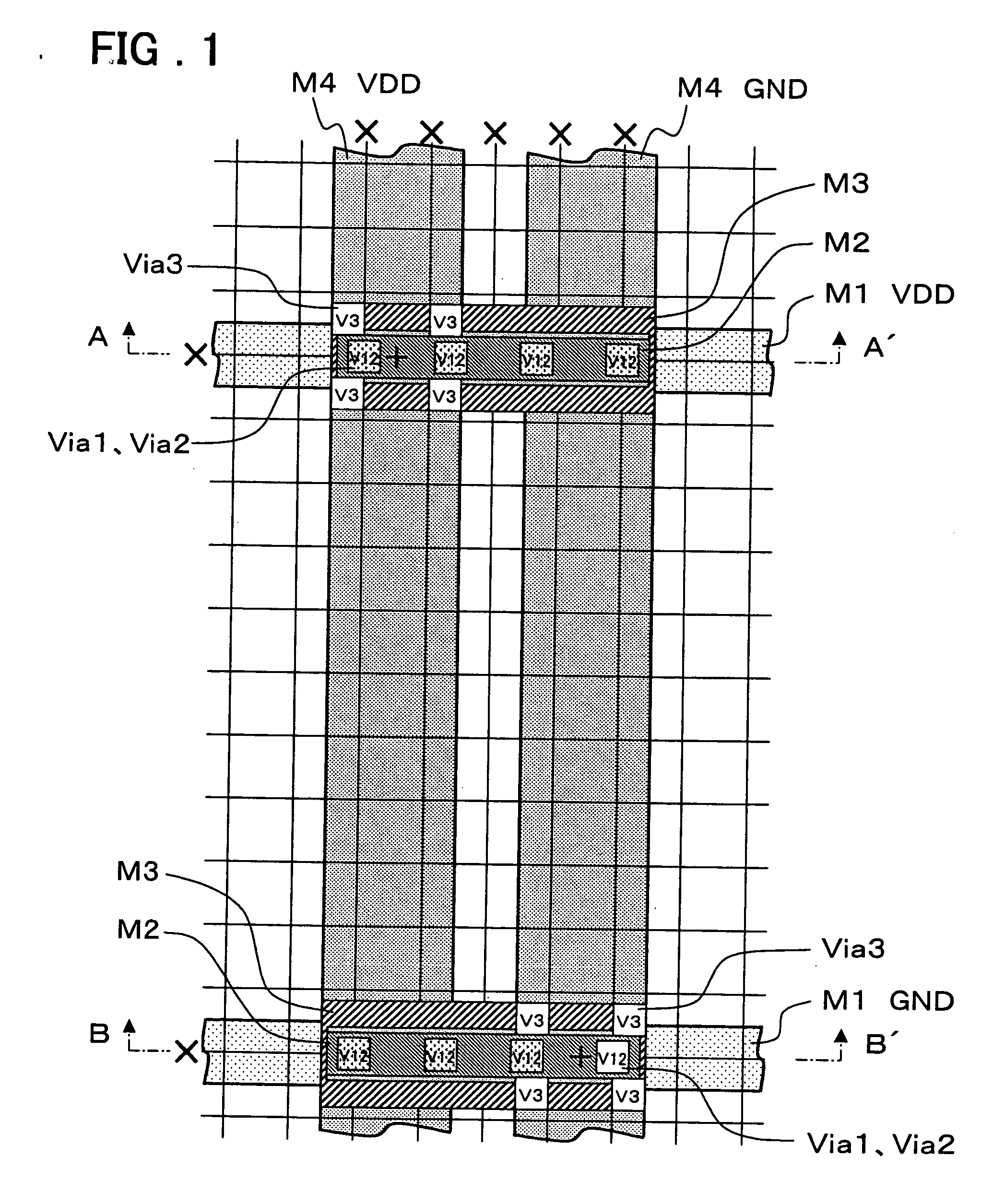
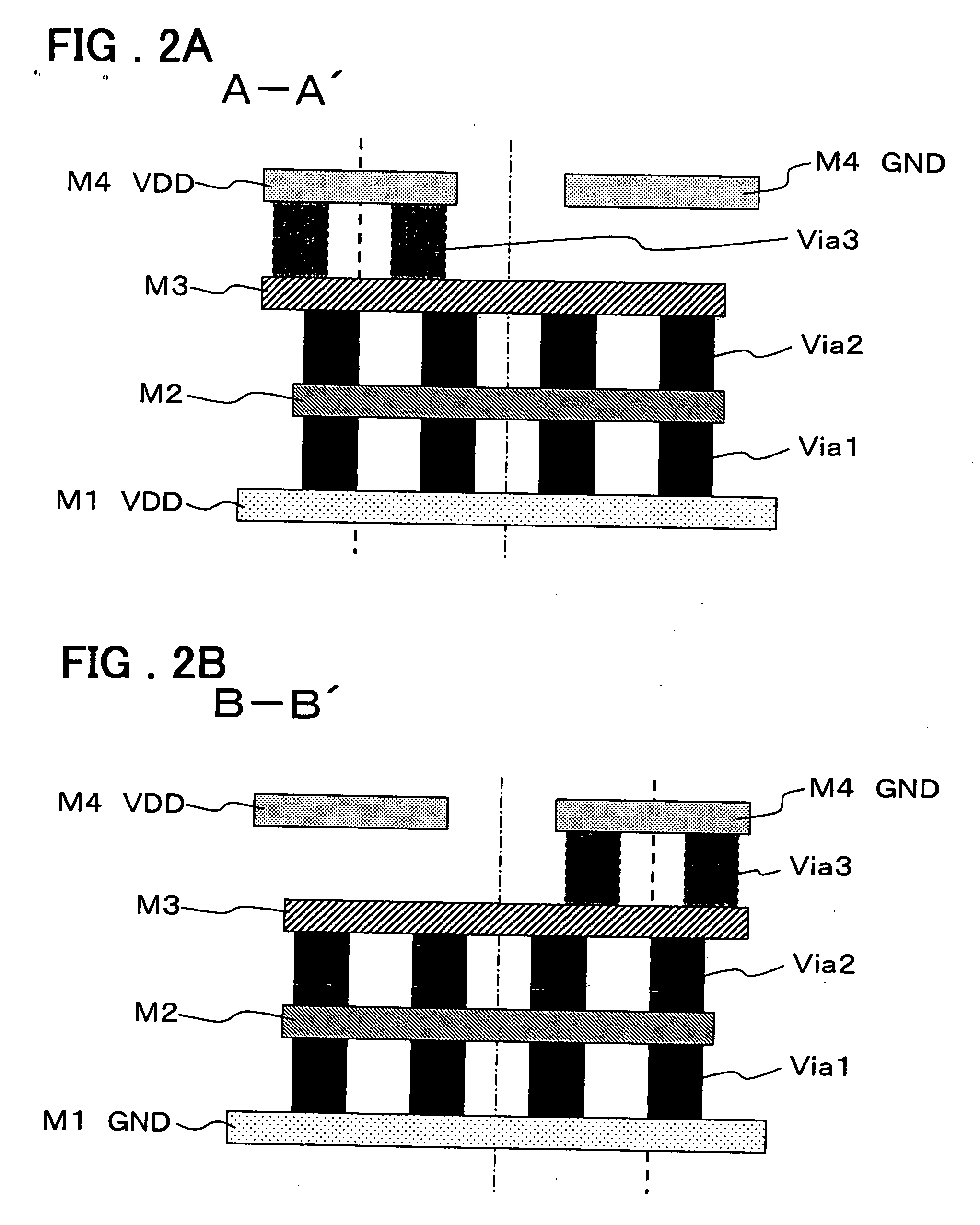
[0038] (First Embodiment)

[0039] A first embodiment of the present invention will be described with reference to the drawings. FIG. 1 is a partial plan view schematically illustrating the wiring structure of a semiconductor integrated circuit according to a first embodiment of the present invention, and FIGS. 2A and 2B show partial sectional views schematically illustrating the wiring structure of the semiconductor integrated circuit according to the first embodiment, in which FIGS. 2A and 2B are partial sectional views taken along lines A-A′ and B-B′, respectively. In FIGS. 2A and 2B, Via 3 is illustrated to facilitate the description although it is not actually visible in this cross section. Further, the grid-like lines in FIG. 1 are wiring tracks (a wiring grid) and serve as auxiliary lines when the wiring structure of the semiconductor integrated circuit is designed. Furthermore, the “+” symbols indicate the centers of via units comprising vias (Vias 3), which connect to the uppe...

second embodiment

[0043] (Second Embodiment)

[0044] A second embodiment of the present invention will now be described with reference to the drawings. FIG. 4 is a partial plan view schematically illustrating the wiring structure of a semiconductor integrated circuit according to a second embodiment of the present invention, and FIGS. 5A and 5B show partial sectional views schematically illustrating the wiring structure of the semiconductor integrated circuit according to the second embodiment, in which FIGS. 5A and 5B are partial sectional views taken along lines C-C′ and D-D′, respectively. The grid-like lines in FIG. 4 are wiring tracks (a wiring grid) and serve as auxiliary lines when the wiring structure of the semiconductor integrated circuit is designed. Furthermore, the “+” symbols indicate the centers of via units comprising vias (Vias 3), which connect to the uppermost wiring layer (M4), as seen from the direction normal to the plane, and the “X” symbols indicate the wiring tracks superposed ...

third embodiment

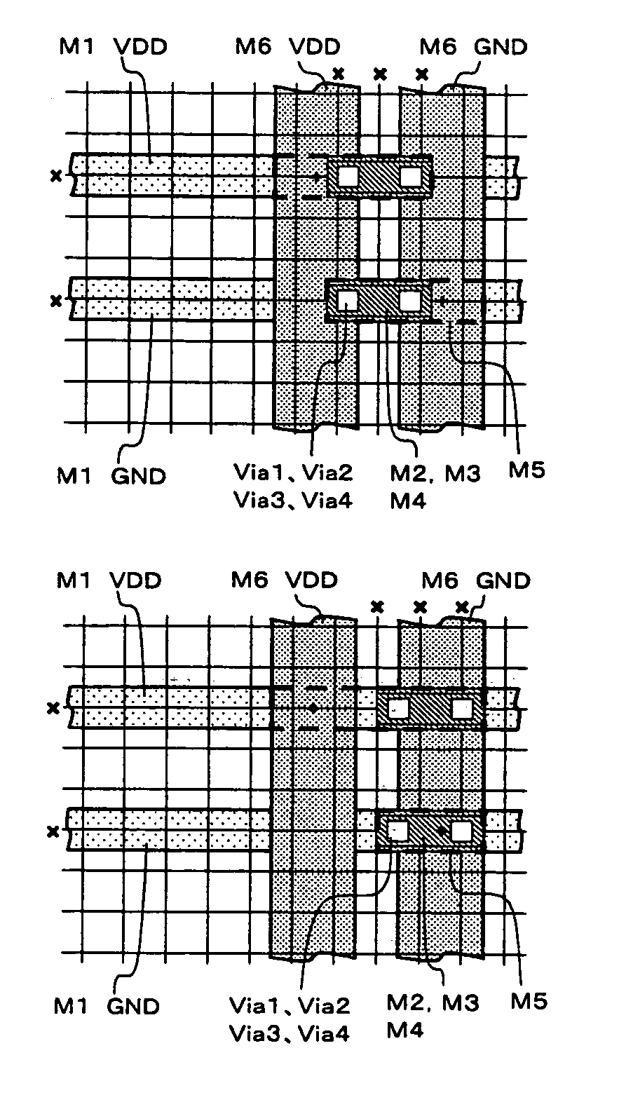
[0045] (Third Embodiment)

[0046] A third embodiment of the present invention will now be described with reference to the drawings. FIG. 6 is a partial plan view schematically illustrating the wiring structure of a semiconductor integrated circuit according to a third embodiment of the present invention, and FIGS. 7A and 7B show partial sectional views schematically illustrating the wiring structure of the semiconductor integrated circuit according to the third embodiment, in which FIGS. 7A and 7B are partial sectional views taken along lines E-E′ and F-F′, respectively. The grid-like lines in FIG. 6 are wiring tracks (a wiring grid) and serve as auxiliary lines when the wiring structure of the semiconductor integrated circuit is designed. Furthermore, the “+” symbols in FIG. 6 indicate the centers of via units comprising vias (Vias 4), which connect to an uppermost wiring layer (M5), as seen from the direction normal to the plane, and the “X” symbols indicate the wiring tracks superp...


PUM


Abstract

An intermediate wiring layer, lowermost vias and uppermost vias of a semiconductor integrated circuit are disposed within a zone of wiring tracks, which are superposed by wiring traces of an uppermost wiring layer and wiring traces of a lowermost wiring layer, as seen from the direction normal to the plane. The lowermost vias are disposed so as to fit in a 4-row, 1-column rectangle, and the uppermost vias are disposed so as to fit in a 2-row, 2-column rectangle. The center of a via unit, which comprises the uppermost vias, as seen from the direction normal to the plane is disposed at the intersecting portion of the lowermost wiring layer and uppermost wiring layer. The center of a via unit, which comprises the lower vias, as seen from the direction normal to the plane is offset by a prescribed amount from the center of the via unit, which comprises the uppermost vias, as seen from the direction normal to the plane.

Description

FIELD OF THE INVENTION [0001] This invention relates to a semiconductor integrated circuit having a wiring structure in which three or more wiring layers each having a single pair of wiring traces of different potentials on a semiconductor substrate are connected by vias, a layout method, apparatus and program. More particularly, the invention relates to a semiconductor integrated circuit, layout method, apparatus and program that are capable of suppressing a decline in wiring ability. BACKGROUND OF THE INVENTION [0002] In a semiconductor integrated circuit such as an LSI chip, it is necessary to strengthen the structure of the power wiring internally of the semiconductor integrated circuit in order to prevent malfunction caused by a fluctuation in delay ascribable to a voltage drop (IR drop), or failure due to electromigration (EM). Strengthening of the power wiring structure is achieved by adjusting wiring width and the number of vias. [0003] An example of prior art that contempla...

Claims


Application Information

Patent Timeline
IPC IPC(8): H01L27/10
CPCG06F17/5077H01L23/5286H01L27/0207H01L2924/0002H01L2924/00G06F30/394
Inventor TAMIYA, MASAYUKI
Owner RENESAS ELECTRONICS CORP
Why Eureka
Try Eureka