High frequency and wide band impedance matching via

a wide band impedance and high frequency technology, applied in the field of conductive vias, can solve the problems of system instability, system damage, and reduced flexibility in circuit application, and achieve the effect of promoting electric characteristics of the structur

Inactive Publication Date: 2006-07-20
IND TECH RES INST
View PDF9 Cites 38 Cited by
  • Summary
  • Abstract
  • Description
  • Claims
  • Application Information

AI Technical Summary

Benefits of technology

[0008] The structure has two ground vias, which are symmetrically sited around the signal via to be similar to a coplanar waveguide, and further, the structure has at least two ground vias which are symmetr

Problems solved by technology

Once the number of layers of the PCB is increased, it results such serious interference that signal transmission lines must be through each layer.
Further, since the prevailing trend in electronic products is high frequency, high transmission speed and a higher requirement for accuracy of the transmission impedance and efficiency of the signal transmission, the impedance dis-matching results in the signal bounce to cause many problems.
In light cases, the system will work unstable, and in serious cases, the system will be damaged.
However, the circuitry design for the conventional PCB is

Method used


Image

  • High frequency and wide band impedance matching via
  • High frequency and wide band impedance matching via
  • High frequency and wide band impedance matching via

Examples


first embodiment

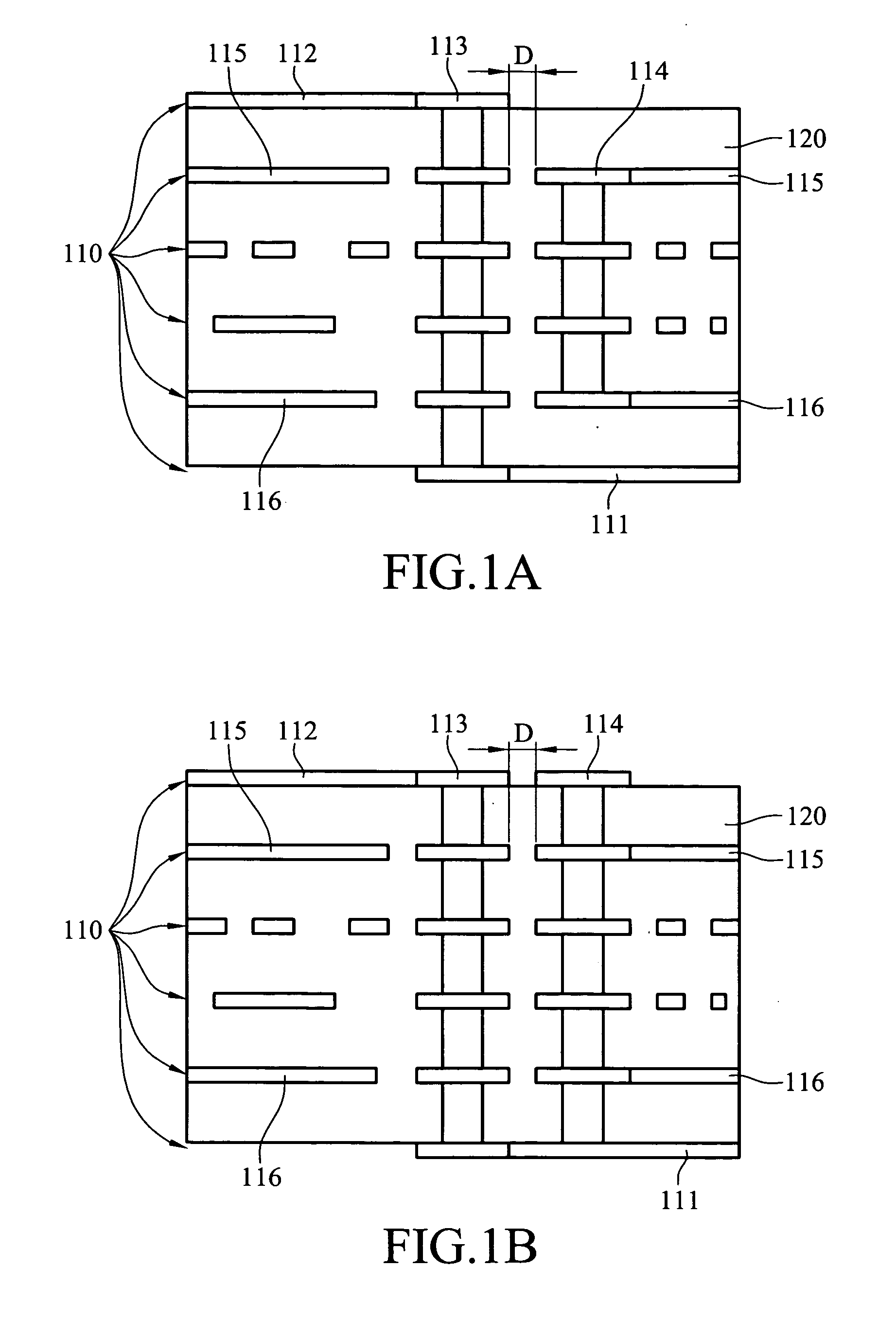
[0021] In an embodiment, the multi-layer printed circuit board is a combination of several insulation layers and several circuit layers, which are stacked staggeredly. Refer to FIG. 1A, which is a cross-section of a first embodiment according to the invention. A six-layer printed circuit board, for example, has six circuit layers 110, which are separated by insulation layers 120. The circuit layer 110 may be a signal transmission trace or a ground layer. The signal and the ground vias 113, 114 are substantially perpendicular to first and second signal transmission traces 111, 112, and first and second ground layers 115, 116. The first signal transmission trace 111 is sited on the bottom circuit layer 110, as a first surface of the substrate, the second signal transmission trace 112 is sited on the top circuit layer 110, as a second surface of the substrate, and the several insulation layers 120 separate them. The first signal transmission trace 111 is connected to the second signal ...

fourth embodiment

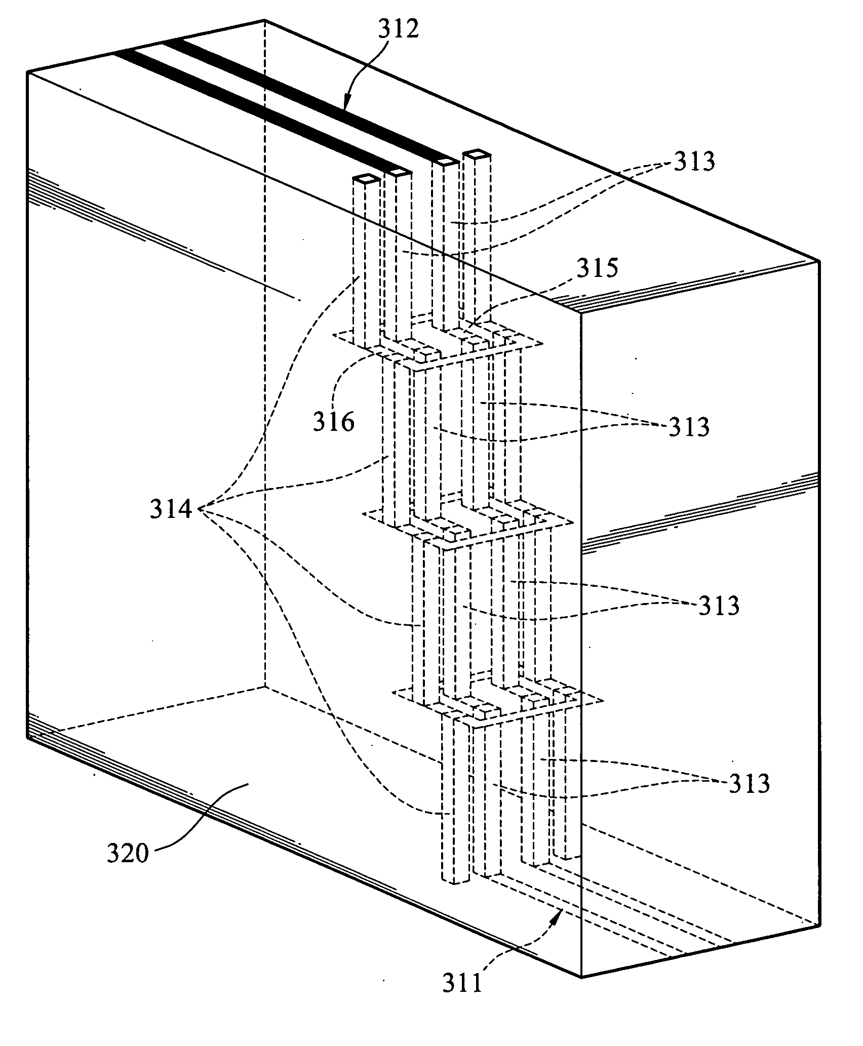
[0023] Further, the structure according to the invention is applied in the signal transmission for differential pairs. Refer to FIG. 3A, which is three-dimensional structures of a fourth embodiment according to the invention. In this embodiment, the structure comprises a first signal transmission differential pair 311, a second signal transmission differential pair 312, a pair of signal vias, several ground vias 314 and a conductor portion. In this case, the conductor portion is a hollow conductor portion 316. The pair of ground vias 314 is substantially perpendicular to the first and the second signal transmission differential pairs 311, 312. The first and the second signal transmission differential pairs 311, 312 are separated with an insulation layer 320, and the first and the second signal transmission differential pairs 311, 312 are connected by several signal vias. The signal vias comprise several vertical signal vias 313 and several plane conductor traces 315. The vertical si...


PUM


Abstract

A high frequency and wide band impedance matching via is provided. As an application to multi-layer printed circuit boards, for example, the multi-layer circuit board has several signal transmission traces, several ground layers, signal transmission vias and ground vias. The signal transmission traces and the ground layers are sited on different circuit layers, and each signal transmission trace is opposite to one of the ground layers. The signal transmission vias are connected between the signal transmission traces. The ground vias are connected between the ground layers. The ground vias are opposite to the signal transmission vias, and the ground vias corresponding to the signal transmission vias are sited to stabilize the characteristic impedance of the transmission traces.

Description

BACKGROUND [0001] This Non-provisional application claims priority under 35 U.S.C. § 119(a) on Patent Application No(s). 94101223 filed in Taiwan on Jan. 14, 2005, the entire contents of which are hereby incorporated by reference. FIELD OF INVENTION [0002] The invention relates to a conductive via to be applied to several substrates, such as multi-layer circuit boards, low temperature co-fired ceramics (LTCCs), integrated circuits (ICs), thick-film ceramics, thin-film ceramics or silicon-on-glass substrate processes, and more particular, to a high frequency and wide band impedance matching via. DESCRIPTION OF THE RELATED ART [0003] In products related to electronic systems, such as the multi-layer circuit boards, LTCCs, ICs, thick-film ceramics, thin-film ceramics and silicon-on-glass substrate processes, the printed circuit board (PCB), which supports electronic components generally, is a plan substrate which was made up of glass fibers and on which conductive circuitry was printed...

Claims


Application Information

Patent Timeline
IPC IPC(8): H03H7/38
CPCH01L23/66H01L2223/6616H01L2223/6638H01L2924/09701H01L2924/3011H01P5/02H05K1/0222H05K1/0245H05K1/0251H05K1/115H05K1/116H05K3/429H05K2201/09236H05K2201/09454H05K2201/09618H05K2201/09627H05K2201/09809H05K2201/09845H01L2924/0002H01L2924/00
Inventor JOW, UEI-MINGWENG, CHING-LIANGLAI, YING-JIUNNCHEN, CHANG-SHENG
Owner IND TECH RES INST
Why Eureka
Try Eureka