Method of creating core-tile-switch mapping architecture in on-chip bus and computer-readable medium for recording the method

a technology of core-tile switch and mapping architecture, which is applied in the direction of roads, instruments, roads, etc., can solve the problems of increasing the burden on transmission and reception of data among the cores, reducing the size of a product, and reducing the development time and cos

Active Publication Date: 2006-07-20
SAMSUNG ELECTRONICS CO LTD
View PDF3 Cites 119 Cited by
  • Summary
  • Abstract
  • Description
  • Claims
  • Application Information

AI Technical Summary

Benefits of technology

[0027] The bandwidth of an arbitrary link is equal to or smaller than the maximum bandwidth that can be sim

Problems solved by technology

Such integration may reduce the size of a product and decrease the development time and cost.
Sometimes, blocks within a functional system-on-chip require a high data bandwidth, which increases the burden on transmission and reception of data among the cores.
For example, in the case of a system-on-chip including a large-capacity on-chip memory and a controller for processing audio and video signals or a CODEC, considerable time and cost are required for designing the architecture of data transmission and reception between the functional blocks in the chip.

Method used


Image

  • Method of creating core-tile-switch mapping architecture in on-chip bus and computer-readable medium for recording the method
  • Method of creating core-tile-switch mapping architecture in on-chip bus and computer-readable medium for recording the method
  • Method of creating core-tile-switch mapping architecture in on-chip bus and computer-readable medium for recording the method

Examples


Embodiment Construction

[0036] Hereinafter, embodiments of the present invention will be described in detail with reference to the appended drawings. Like reference numbers refer to like components throughout the drawings.

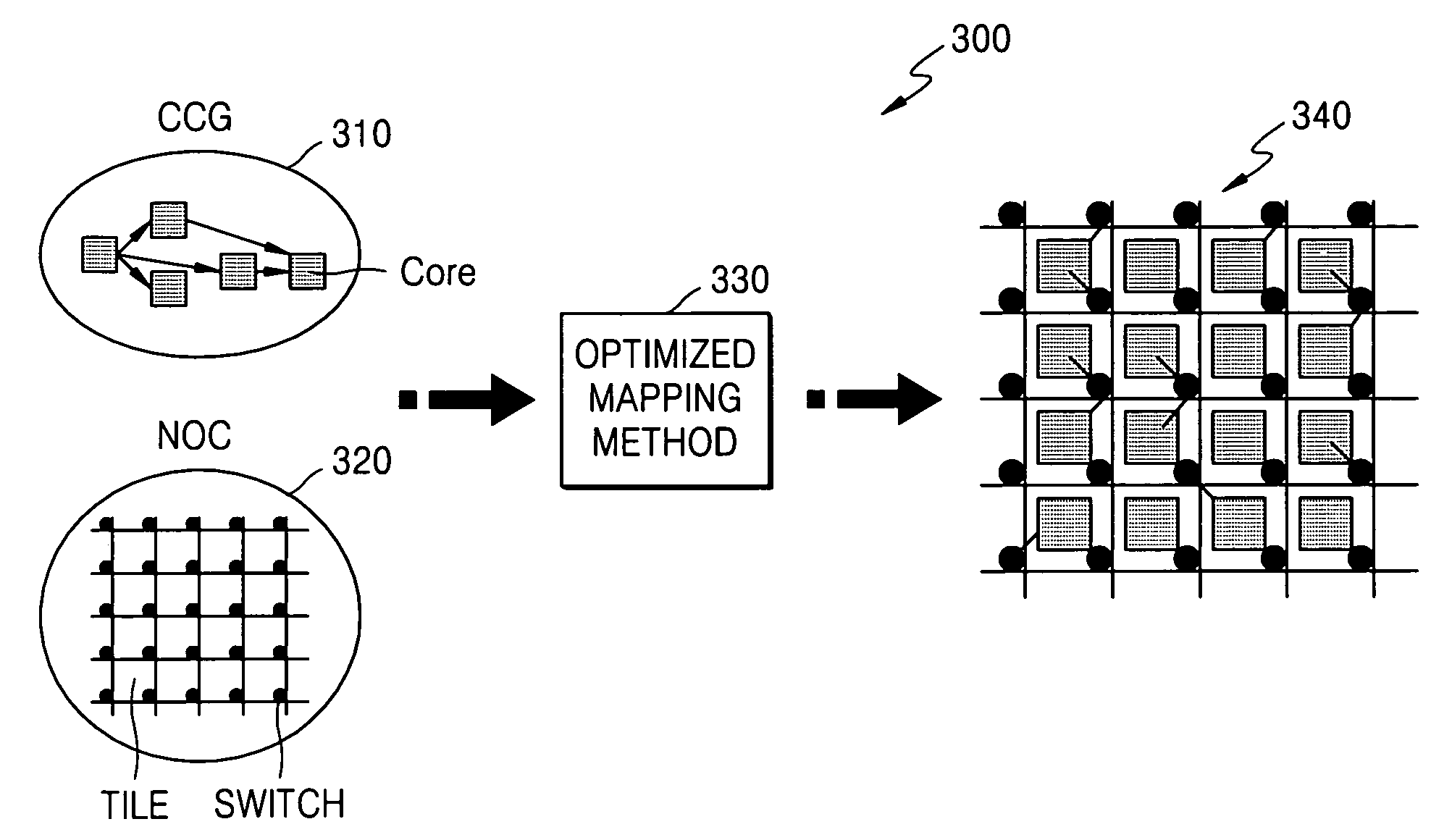
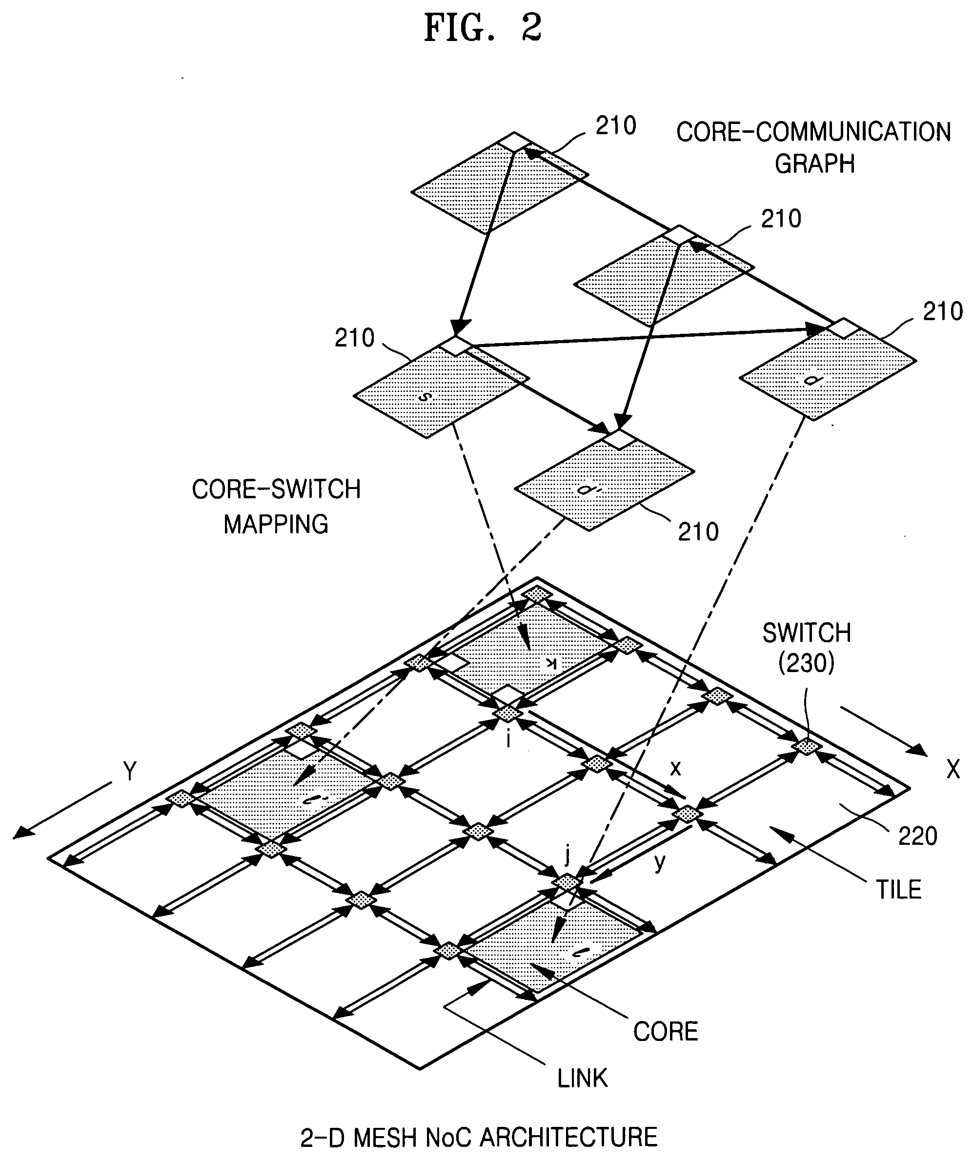
[0037]FIG. 3 is a diagram for explaining a method of creating a core-tile-switch mapping architecture according to an embodiment of the present invention. FIG. 4 is a flowchart illustrating the method of creating the core-tile-switch mapping architecture according to an embodiment of the present invention.

[0038] Referring to FIGS. 3 and 4, first, a core communication graph (CCG) 310 representing the connection relationship between arbitrary cores is created (operation 410). The connection relationship between arbitrary cores can be set by a designer of a system-on-chip. In the following descriptions, for the convenience of description, it is assumed that an arbitrary core s is connected to another arbitrary core d. Then, a network-on-chip (NOC) architecture 320 including a plurality of ...


PUM


Abstract

There are provided a method of creating an optimized core-tile-switch mapping architecture in an on-chip bus and a computer-readable recording medium for recording the method. The core-tile-switch mapping architecture creating method includes: creating a core communication graph representing the connection relationship between arbitrary cores; creating a Network-on-chip (NOC) architecture including a plurality of switches, a plurality of tiles, and a plurality of links interconnecting the plurality of switches; and mapping the cores to the tiles using a predetermined optimized mapping method to thereby create the optimized core-tile-switch mapping architecture. The optimized mapping method includes first, second, and third calculating steps. According to the optimized core-tile-switch mapping architecture creating method and the computer-readable recording medium for recording the method, since the hop distance between cores is minimized, it is possible to minimize energy consumption and communication delay time in an on-chip bus. Furthermore, the optimized mapping architecture presents a standard for comparing the optimization of other mapping architectures.

Description

REFERENCE TO PRIORITY APPLICATION [0001] This application claims the benefit of Korean Patent Application No. 2005-0001123, filed on Jan. 6, 2005, in the Korean Intellectual Property Office, the disclosure of which is hereby incorporated herein by reference. FIELD OF THE INVENTION [0002] The present invention related to integrated circuit manufacturing methods and, more particularly, to methods of designing high density integrated circuit chips with multiple functional logic blocks. BACKGROUND OF THE INVENTION [0003] Conventional chip sets, where separate chips each execute their own functions, are evolving toward system-on-chip technology, where various functional blocks are integrated on a single chip. The system-on-chip may integrate a variety of functional blocks on a single chip, including a microprocessor, an on-chip memory, an audio and video controller, a CODEC, a digital signal processor. Such integration may reduce the size of a product and decrease the development time an...

Claims


Application Information

Patent Timeline
IPC IPC(8): G06F17/50
CPCG06F17/5068G06F30/39E01C19/1068
Inventor RHEE, CHAE-EUN
Owner SAMSUNG ELECTRONICS CO LTD
Why Eureka
Try Eureka