Coating and developing system and coating and developing method

a technology of developing system and developing method, applied in the direction of printers, instruments, photosensitive materials, etc., can solve the problems of large processing block, large area, and inability to work, so as to reduce the need for space and simplify the software

Active Publication Date: 2006-07-27
TOKYO ELECTRON LTD
View PDF12 Cites 24 Cited by
  • Summary
  • Abstract
  • Description
  • Claims
  • Application Information

AI Technical Summary

Benefits of technology

[0013] The present invention has been made under such circumstances and it is therefore an object of the present invention to provide techniques for forming antireflection films over and under a resist film, capable of reducing necessary space. Another object of the present invention is to provide techniques capable of dealing with either of a case where an antireflection film is formed and a case where any antireflection film is not formed and of simplifying software.

Problems solved by technology

Since carrying programs to be produced according to the carrying schedule are originally complex, work for producing a carrying program for each of desired resist films is very complex and troublesome and such work is practically impossible.
When units including the coating unit, the heating unit and the cooling unit are installed in the same processing block, the processing block is inevitably large and occupies a large area.
However, the same carrying system operates to carry a wafer W to the coating unit for forming a resist film before the exposure process, to carry a wafer to an antireflection film forming unit for forming the antireflection film and to carry a wafer coated with an exposed resist film to the developing unit after exposure, it is difficult to operate the exposure system at a high throughput.

Method used


Image

  • Coating and developing system and coating and developing method
  • Coating and developing system and coating and developing method
  • Coating and developing system and coating and developing method

Examples


second embodiment

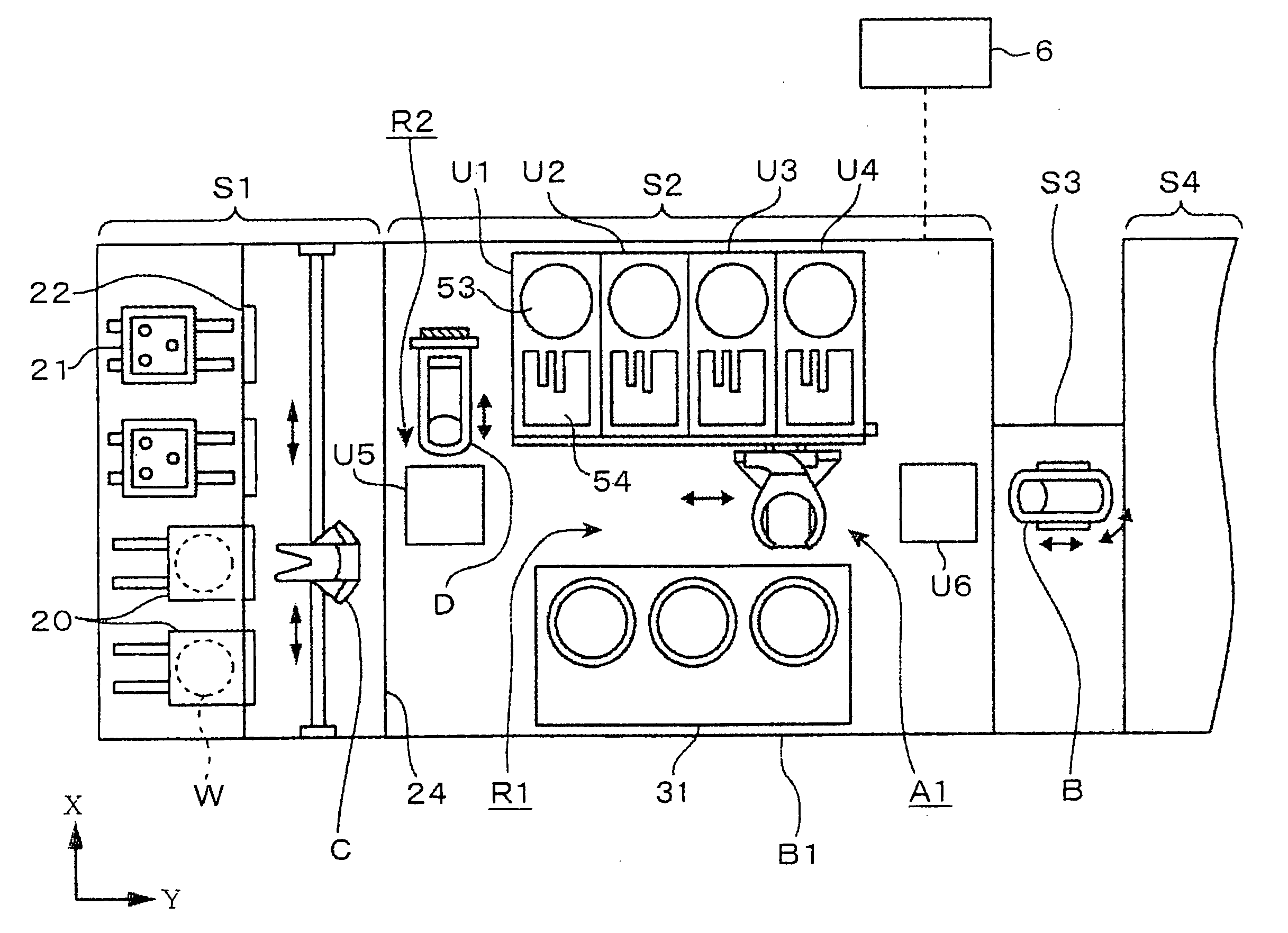
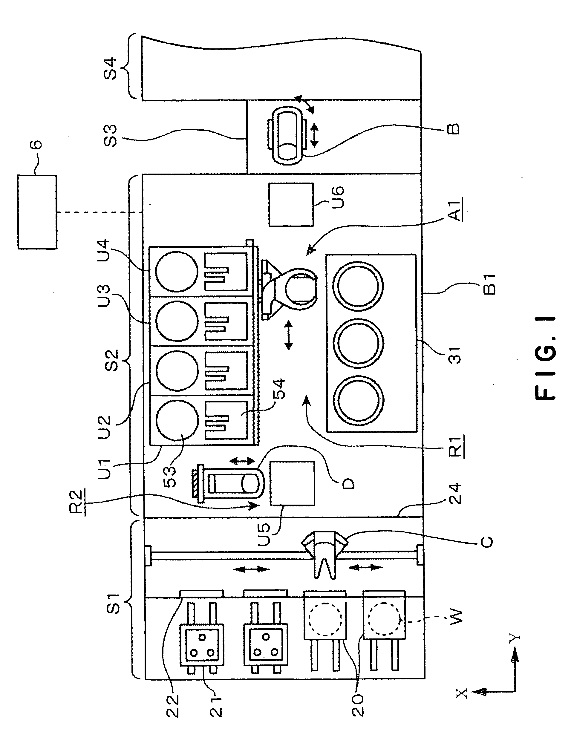
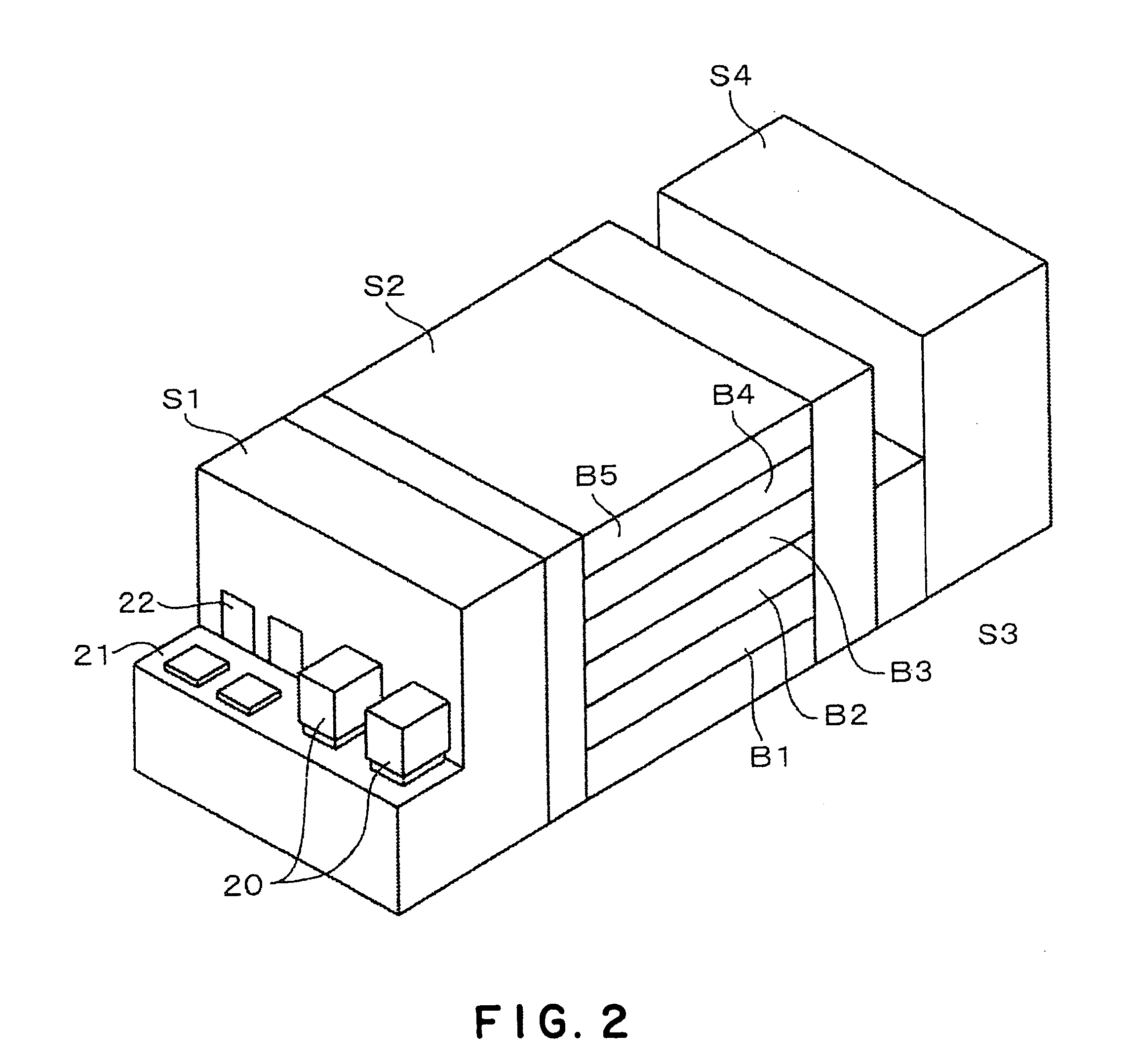
[0109] A coating and developing system in a second embodiment according to the present invention will be described with reference to FIG. 11. This coating and developing system is combined with an exposure system S4 which carries out an immersion exposure process which forms a liquid layer on a surface of the wafer W, includes an auxiliary block S5 interposed between a processing block S2 and an interface block S3, and is provided additionally with a film forming unit block, not shown, including a water-repellent protective film forming unit, for forming a water-repellent protective film on a second antireflection film or a resist film, disposed, for example, on a BCT layer B5. The water-repellent protective film forming unit is a liquid-processing unit to deal with immersion exposure. The water-repellent protective film forming unit forms a protective film capable of preventing a resist film from being impregnated with a liquid for immersion exposure. The unit block including the w...

third embodiment

[0135] A resist pattern forming system in a third embodiment according to the present invention has the following construction illustrated in FIGS. 12 to 17. The resist pattern forming system has an auxiliary block S5. The auxiliary block S5 is provided with water-repellent protective film forming units (ITC) (hereinafter, referred to as “protective film forming units (ITC)”), and water-repellent protective film removing units (ITR) (hereinafter referred to as “protective film removing units (ITR)”). The protective film forming unit (ITC) forms a protective film on a resist film to prevent the penetration of a liquid into the resist film. The protective film removing unit (ITR) removes the water-repellent protective film formed on the resist film. An interface unit S3 is provided with cleaning units RD for cleaning a wafer before and after immersion exposure.

[0136] Immersion exposure will be briefly described. Immersion exposure exposes a surface of a substrate coated with a liquid ...

first embodiment

[0158] An immersion exposure process and a cleaning process to be carried out by the resist pattern forming system are similar to those to be carried out by, for example, the The wafer W is carried from the carrier block S1, along a carrying route sequentially passing the BCT layer B5, the COT layer B4 and the TCT layer B3. Then, the wafer W is carried along a route sequentially passing the first transfer stage TRS2 of the shelf unit U5, the transfer arm D2, the main arm A2 of the DEV layer B2, the second transfer stage TRS7 of the shelf unit U6, the fourth transfer arm F1 of the auxiliary block S5, the protective film forming unit 401 of the shelf unit U8, the transfer stage TRS12 of the shelf unit U7, the interface arm B of the interface block S3, and the exposure system S4. The wafer W processed by exposure is carried along a route sequentially passing the interface arm B of the interface block S3, the cleaning unit 403, the interface arm B, the transfer stage TRS11 of the shelf...


PUM


Abstract

A coating and developing system includes a resist film forming unit block and antireflection film forming unit blocks stacked up in layers to form a resist film and an antireflection film underlying the resist film and an antireflection film overlying the resist film in a small space. The coating and developing system is capable of coping with either of a case where antireflection films are formed and a case where any antireflection film is not formed and needs simple software. Film forming unit blocks, namely, a TCT layer B3, a COT layer B4 and a BCT layer B5, and developing unit blocks, namely, DEV layers B1 and B2, are stacked up in layers in a processing block S2. The TCT layer B3, the COT layer B4 and the BCT layer B5 are used selectively in the case where antireflection films are formed and the case where any antireflection film is not formed. The coating and developing system is controlled by a simple carrying program and simple software.

Description

BACKGROUND OF THE INVENTION [0001] 1. Field of the Invention [0002] The present invention relates to a coating and developing system for applying a liquid resist to a surface of a substrate, such as a semiconductor wafer or a LCD substrate, namely, a glass substrate for a liquid crystal display, to coat the surface with a resist film and developing the exposed resist film, and a coating and developing method. [0003] 2. Description of the Related Art [0004] In a manufacturing process for manufacturing semiconductor devices or LCD panels, a resist pattern is formed on a substrate by a photolithographic process. The photolithographic process includes a series of steps of forming a resist film on a substrate, such as a semiconductor wafer (hereinafter, referred to simply as “wafer”) by applying a liquid resist to the surface of the substrate, exposing the resist film to light through a photomask, and developing the exposed resist film to form a desired resist pattern. [0005] Generally, ...

Claims


Application Information

Patent Timeline
Patent Type & Authority Applications(United States)
IPC IPC(8): G03D5/00
CPCH01L21/00H01L21/6715H01L21/67178H01L21/67184H01L21/6719E06B3/7003E06B3/7001
Inventor AKIMOTO, MASAMIHAYASHI, SHINICHIHAYASHIDA, YASUSHIMATSUOKA, NOBUAKIKIMURA, YOSHIOUEDA, ISSEIITO, HIKARU
Owner TOKYO ELECTRON LTD
Why Eureka
Try Eureka