Conductive heat transfer for electrical devices from the solder side and component side of a circuit card assembly
- Summary
- Abstract
- Description
- Claims
- Application Information
AI Technical Summary
Benefits of technology
Problems solved by technology
Method used
Image
Examples
Embodiment Construction
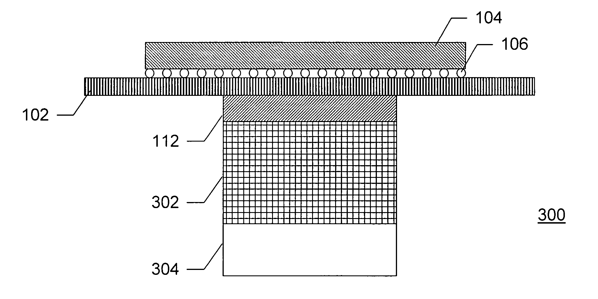
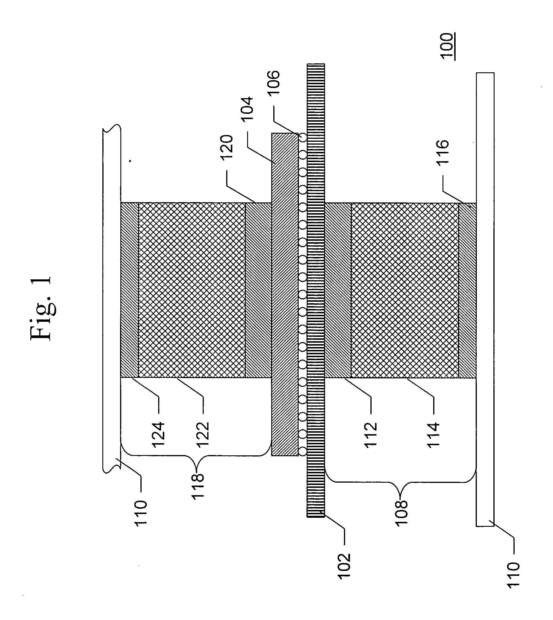
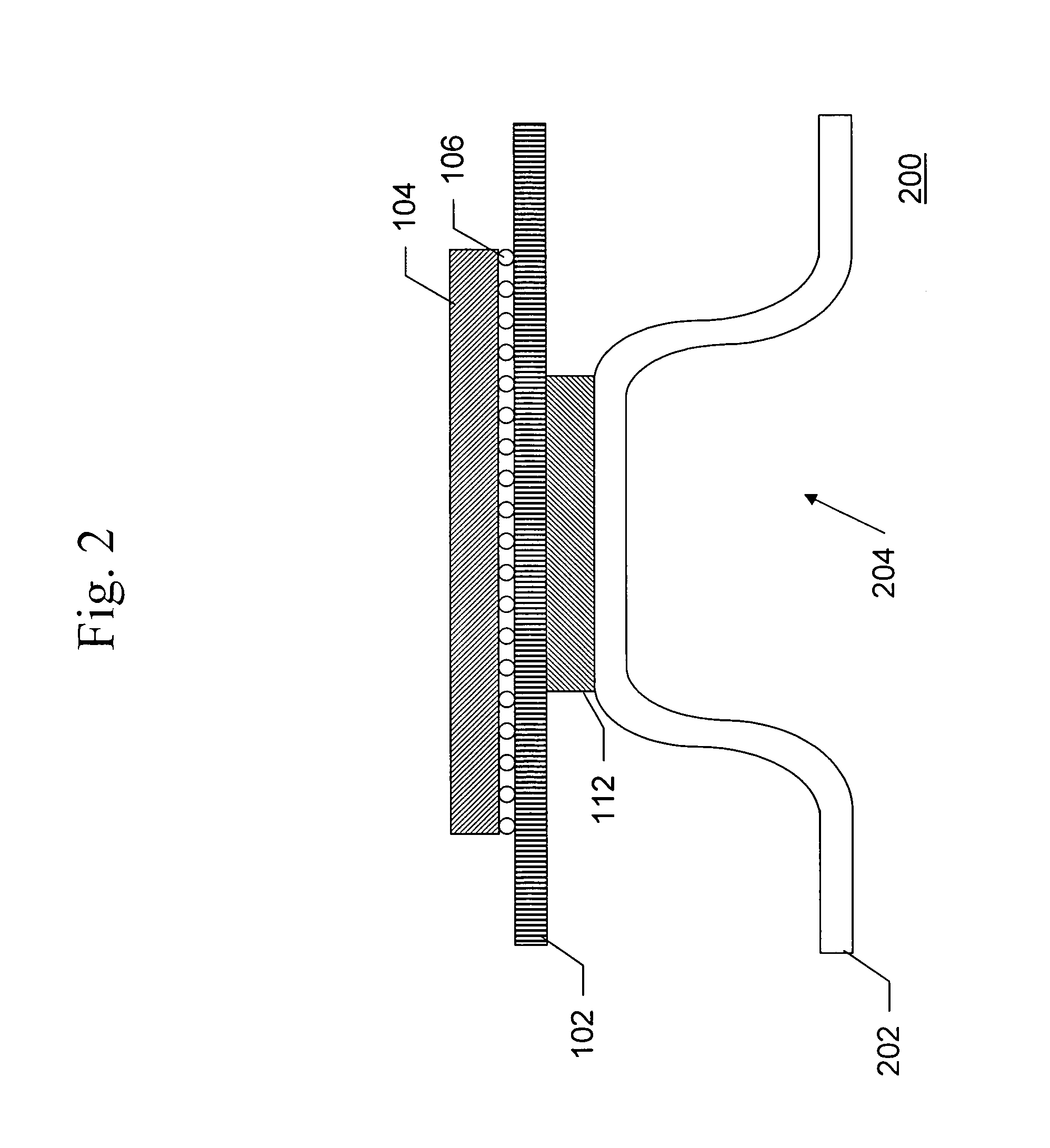
[0017] The present invention employs the backside of the printed circuit board to remove heat from an electrical component. Technology today dictates that electrical components are capable of higher power dissipations. Typically, these high power components are a ball grid array package. Since the package has many solder balls and the printed circuit board (PCB) below it has a large percentage of copper coverage, the circuit board becomes a good conductive heat path. The backside of the PCB is available for heat removal.
[0018] This invention mounts a compliant thermal interface material on the backside of the PCB directly below a high heat dissipating electrical device. The compliant material can be placed directly over small surface mount capacitors and resistors. An optional aluminum block is adhered to the top of the thermal interface material. The opposite face of the optional aluminum block mates to the enclosure. To insure there is no air at the interface between the optional...
PUM
 Abstract
Description
Claims
Application Information


