El device, process for manufacturing the same, and liquid crystal display employing el device

a liquid crystal display and el technology, applied in the field of el (electroluminescence) devices, can solve the problems of illumination light attenuation, complex overall structure of liquid crystal display devices, and increase in number of components, and achieve the effect of avoiding light attenuation and simple structur

Inactive Publication Date: 2006-08-10
UTSUMI TETSUYA +5
View PDF9 Cites 8 Cited by
  • Summary
  • Abstract
  • Description
  • Claims
  • Application Information

AI Technical Summary

Benefits of technology

[0013] The present invention has been made in view of the above problems and requirements, a first object of the present invention is to provide an EL device capable of avoiding light attenuation due to the use of a diffusion plate and diffusing the light sufficiently to conduct uniform illumination while having a simple structure.

Problems solved by technology

However, when the diffusion plate is separately arranged between the liquid crystal panel and the organic EL device, the number of components increases, and the overall structure of the liquid crystal display device becomes complicated.
In addition, there is a problem in that when the illumination light passes through the diffusion plate, the illumination light attenuates.
It is because, in particular, with such an EL device of a bottom emission type as shown in FIG. 13 in which the light emitted from the light emitting layer outgoes through the substrate (transparent substrate) toward the outside, the amount of light capable of outgoing from the substrate toward the outside is limited.
This is because light which does not enter the liquid crystal panel A or which enters the liquid crystal panel A but does not outgo from the panel cannot be utilized for the liquid crystal display device.

Method used


Image

  • El device, process for manufacturing the same, and liquid crystal display employing el device
  • El device, process for manufacturing the same, and liquid crystal display employing el device
  • El device, process for manufacturing the same, and liquid crystal display employing el device

Examples


embodiment 1

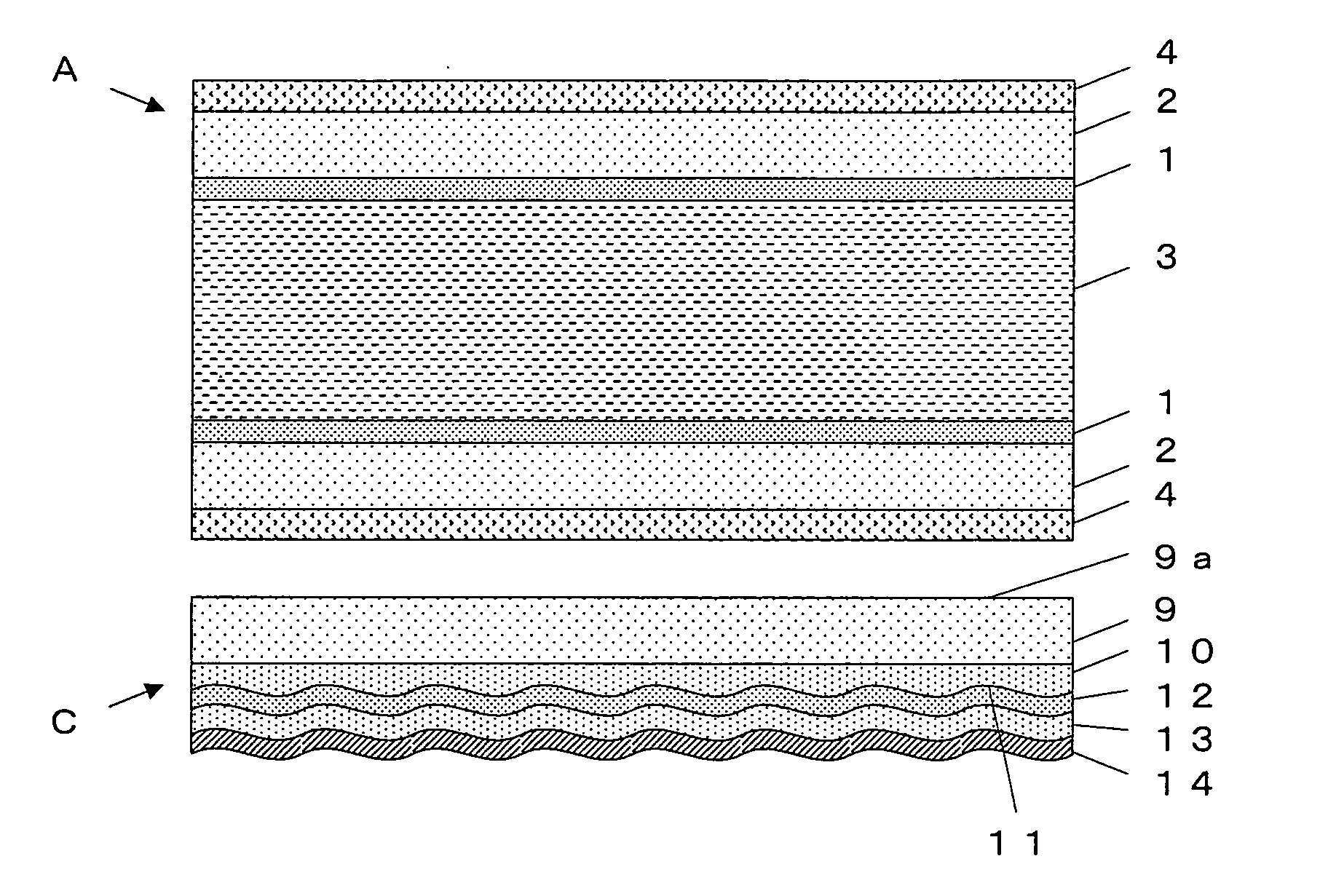
[0044]FIG. 1 shows a cross section of a liquid crystal display device according to Embodiment 1. This liquid crystal display device has a liquid crystal panel A and an organic EL device C disposed at the rear of the liquid crystal panel A as a backlight. The liquid crystal panel A includes a pair of glass substrates 2 disposed in parallel and having transparent electrodes 1 on the surfaces facing each other. Liquid crystal is sealed between the pair of glass substrates 2 to form a liquid crystal layer 3. Further, disposed on outer sides of the pair of glass substrates 2 are deflecting plates 4.

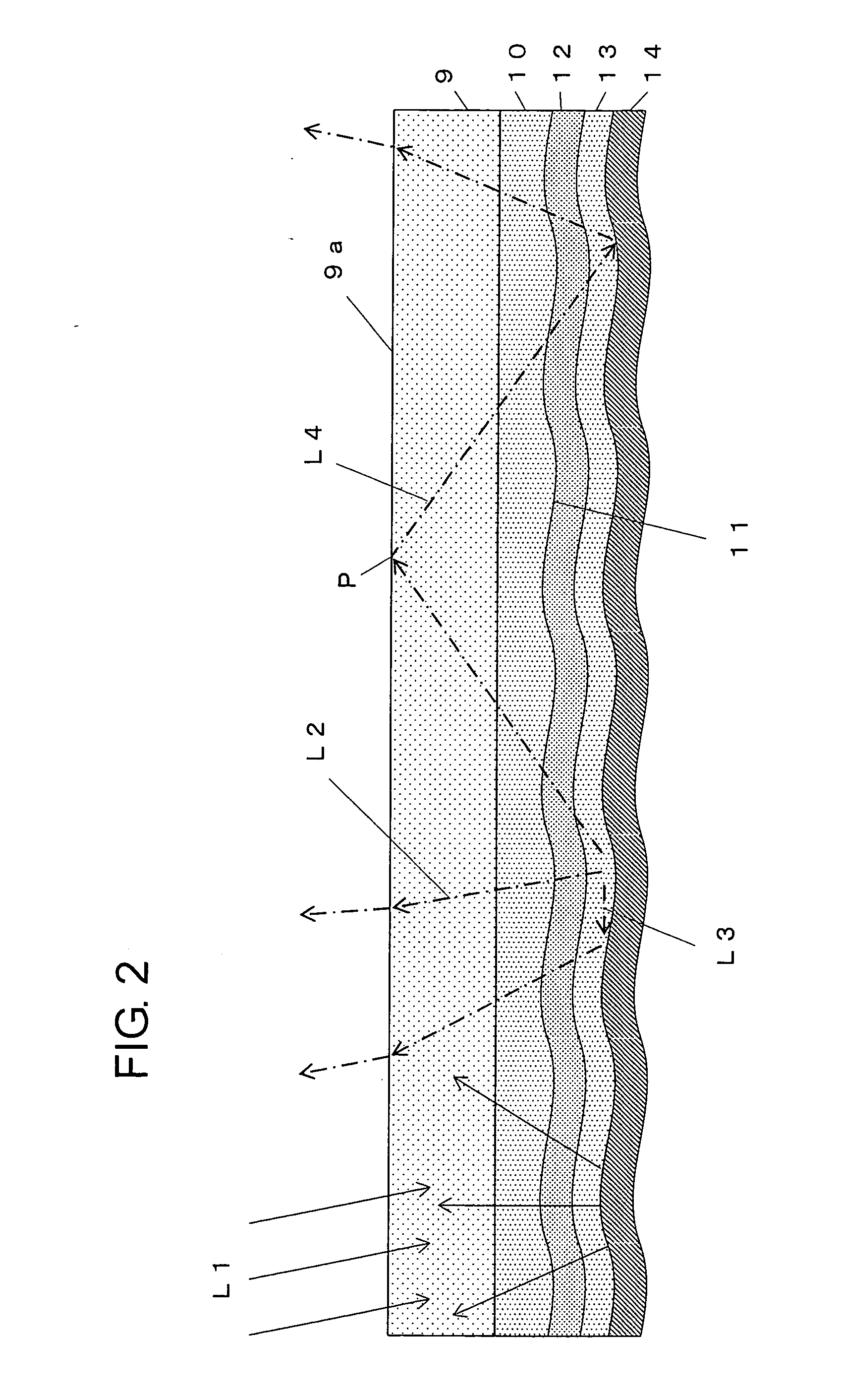
[0045] On the other hand, the organic EL device C includes a planar transparent substrate 9, and formed on this transparent substrate 9 is a transparent layer 10 constituting an intermediate layer of the present invention. The transparent layer 10 has an irregularity surface 11 on which a concave portion and a convex portion are formed at random on a surface thereof opposite to the transparen...

embodiment 2

[0065]FIG. 5 shows a cross section of an organic EL device D according to Embodiment 2. The organic EL device D of Embodiment 2 is obtained by arranging one prism sheet 21 on the light outgoing surface 9a of the transparent substrate 9 of the organic EL device C in Embodiment 1. The prism sheet 21 herein has a plurality of linear convex portions 21a formed in parallel to each other as shown in FIG. 6. Each of the linear convex portions 21a is sharply pointed to have a triangular shape in cross section. This prism sheet 21 is arranged on the light outgoing surface 9a of the transparent substrate 9, therefore the direction of light emitted from the light outgoing surface 9a is refracted according to the shape of the linear convex portions 21a (the angle with respect to the light outgoing surface 9a having a triangular shape in cross section), and the refractive index of the prism sheet 21. For instance, when a prism sheet for refracting the light having an incident angle of about 50° ...


PUM

PropertyMeasurementUnit
incident angleaaaaaaaaaa
thicknessaaaaaaaaaa

Abstract

After entering a transparent substrate 9 of an organic EL device and passing through this substrate 9, an outside light L1 further passes through a transparent layer 10, a transparent electrode 12, and an organic light emitting layer 13 to be reflected by a reflective electrode 14. Herein, the reflective electrode 14 has irregularities and therefore the outside light L1 is diffused and reflected by this at various angles. These reflected lights are further diffused when passing through a boundary between the organic light emitting layer 13 and the transparent electrode 12 and through an irregularity surface 11 of the transparent layer 10, and outgo from the transparent substrate 9 toward a liquid crystal panel. On the other hand, lights L2 to L4 emitted from the organic light emitting layer 13 are diffused when passing through the boundary between the organic light emitting layer 13 and the transparent electrode 12 and through the irregularity surface 11 of the transparent layer 10, and outgo from the transparent substrate 9 toward the liquid crystal panel.

Description

TECHNICAL FIELD [0001] The present invention relates to an EL (electroluminescence) device, and more particularly to an EL device used for a backlight of a liquid crystal display device. [0002] The present invention also relates to a method of manufacturing such an EL device and a liquid crystal display device using the EL device. BACKGROUND ART [0003] Heretofore, EL devices such as an inorganic EL device and an organic EL device have been used for displays and illumination devices. For example, among EL devices used for illumination devices, as shown in FIG. 13, there is an organic EL device B disposed at the rear of a liquid crystal panel A as a backlight and constituting a liquid crystal display device. [0004] The liquid crystal panel A includes a pair of glass substrates 2 disposed in parallel and having transparent electrodes 1 on surfaces facing each other. Liquid crystal is sealed between the pair of glass substrates 2 to form a liquid crystal layer 3. Disposed on outer sides...

Claims


Application Information

Patent Timeline
Patent Type & Authority Applications(United States)
IPC IPC(8): G02F1/1335G02F1/13357H01L51/52H05B33/02H05B33/10H05B33/14
CPCG02F1/133606G02F1/133611G02F2202/02H01L51/5262H01L51/5281H01L2251/5361H10K50/85H10K50/86H05B33/22H05B33/10
Inventor UTSUMI, TETSUYAUTSUMI, TOMOKOFUNADA, MARIKATO, YOSHIFUMIITO, HIRONORITAKEUCHI, NORIHITO
Owner UTSUMI TETSUYA
Why Eureka
Try Eureka