Semiconductor laser module and method for simultaneously reducing relative intensity noise (RIN) and stimulated brillouin scattering (SBS)

a laser module and semiconductor technology, applied in semiconductor lasers, instruments, optical elements, etc., can solve the problems of unfavorable increase in costs and undesirable sbs, and achieve the effect of reducing rin and avoiding sbs

Inactive Publication Date: 2005-09-27
FURUKAWA ELECTRIC CO LTD
View PDF3 Cites 5 Cited by
  • Summary
  • Abstract
  • Description
  • Claims
  • Application Information

AI Technical Summary

Benefits of technology

[0009]Another object of the present invention is to provide an integrated diffraction grating pump module that provides reduced RIN, while also avoiding SBS.

Problems solved by technology

However, in order to increase the data transmission capacity of such single fiber systems, it was necessary to increase the number of optical fibers laid on a transmission route, which resulted in an undesirable increase in costs.
However, the present inventors have discovered that, despite the reduced RIN of the integrated diffraction grating multiple mode pump module, using such a module in the forward excitation system causes undesirable stimulated Brillouin Scattering (SBS) to occur.

Method used


Image

  • Semiconductor laser module and method for simultaneously reducing relative intensity noise (RIN) and stimulated brillouin scattering (SBS)
  • Semiconductor laser module and method for simultaneously reducing relative intensity noise (RIN) and stimulated brillouin scattering (SBS)
  • Semiconductor laser module and method for simultaneously reducing relative intensity noise (RIN) and stimulated brillouin scattering (SBS)

Examples


Embodiment Construction

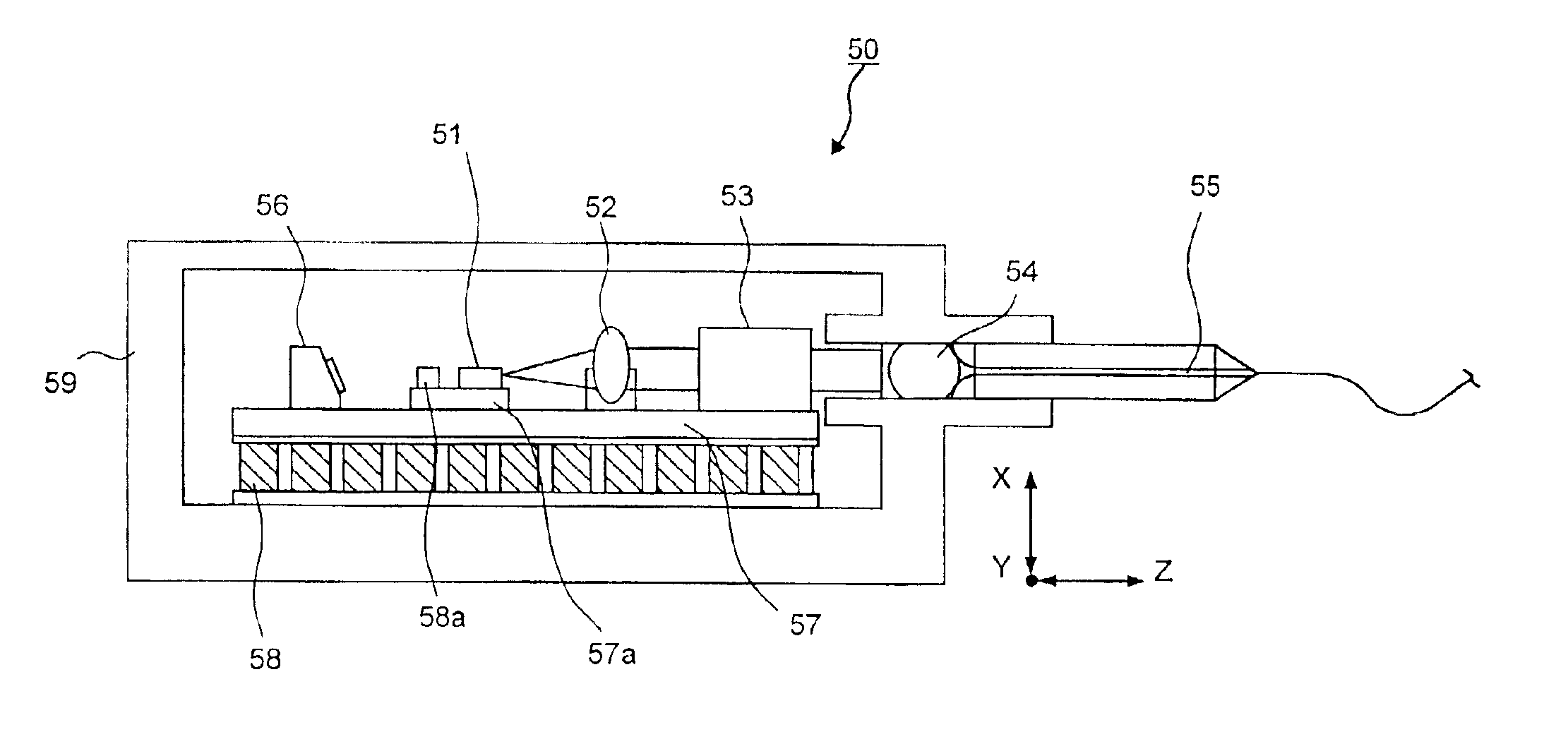
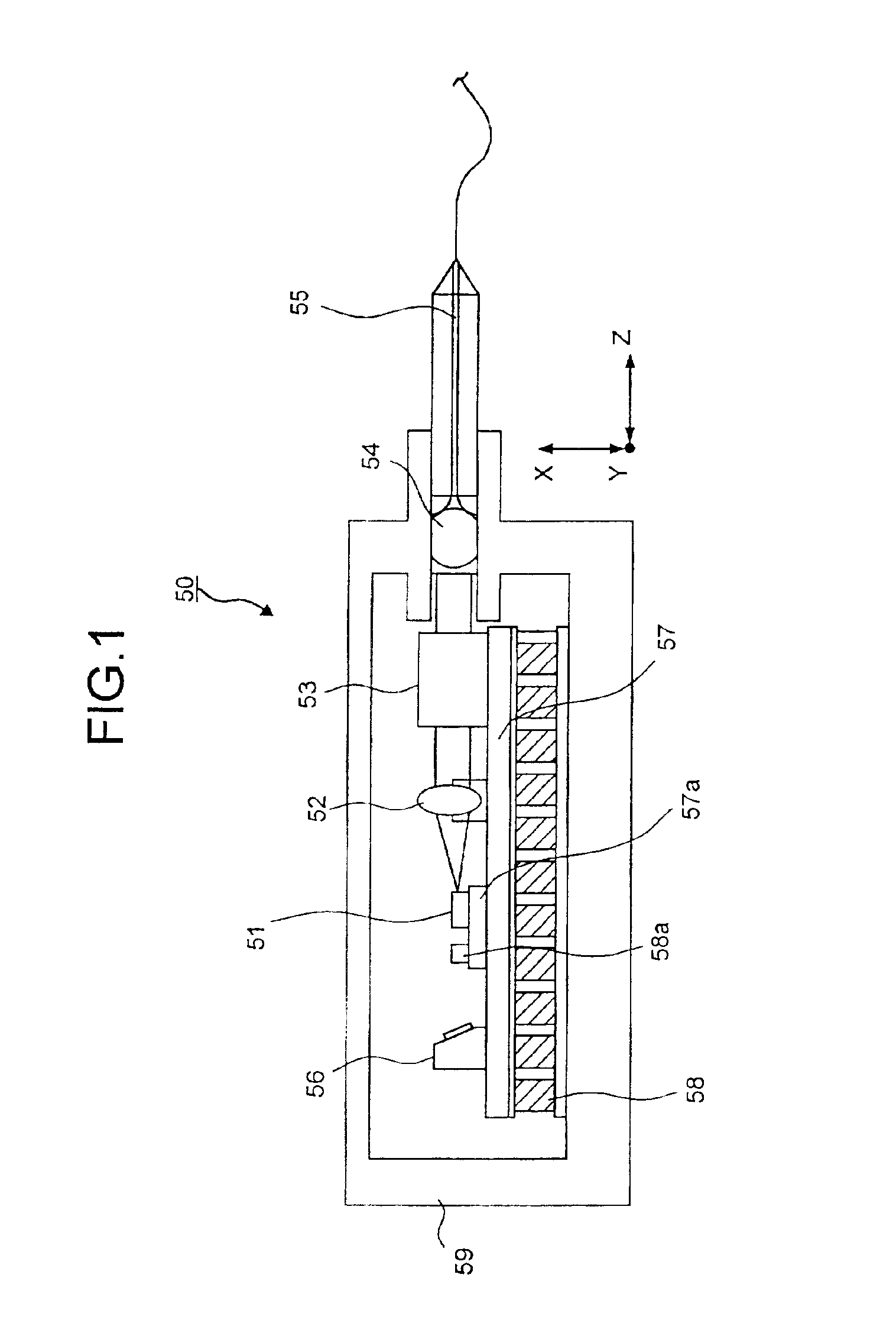
[0043]Referring now to the drawings wherein like elements are represented by the same reference designation throughout, and more particularly to FIG. 1 thereof, there is shown a semiconductor laser module for providing a light source suitable for use as a forward pumping light source in a Raman amplification system, in accordance with the present invention. FIG. 1 is a vertical sectional view illustrating the configuration of a semiconductor laser module according to a first embodiment of the present invention. The semiconductor laser module 50 includes a semiconductor laser device 51, a first lens 52, an internal isolator 53, a second lens 54 and an optical fiber 55. A laser beam irradiated from the semiconductor laser device 51 is guided to optical fiber 55 via first lens 52, internal isolator 53, and second lens 54. The second lens 54 optically couples the laser 51 to the fiber 55 and is provided offset from an optimum position in order to provide a predetermined coupling efficie...


PUM


Abstract

A semiconductor laser module including a semiconductor laser device having an integrated diffraction grating configured to output a multiple mode laser beam in the presence of a driving current, an optical fiber configured to guide the multiple mode laser beam to an output of the laser module, and an optical attenuation device configured to attenuate the multiple mode laser beam by an amount sufficient to provide a predetermined output power from the output of the laser module. The optical attenuation device may be an optical coupling lens offset from an optimum coupling position by an amount sufficient to provide the predetermined output power, or an optical attenuator interrupting the optical fiber and configured to attenuate the multiple mode laser beam by an amount sufficient to provide the predetermined output power. Also, a two fiber Raman amplifier having a super large area (SLA) fiber that provides amplification of the signal based primarily on the forward excitation light can also be used to suppress SBS.

Description

CROSS REFERENCE TO RELATED APPLICATIONS[0001]This application contains subject matter related to U.S. patent application Ser. No. 09 / 832,885 filed on Apr. 12, 2001, Ser. No. 09 / 983,175 filed on Oct. 23, 2001, Ser. No. 09 / 983,249 filed on Oct. 23, 2001. The entire content of each of these applications is incorporated herein by reference.FIELD OF THE INVENTION[0002]The present invention relates generally to semiconductor laser module, and in particular to a semiconductor laser module used as a pumping source for an optical amplifier.BACKGROUND OF THE INVENTION[0003]With the proliferation of multimedia features on the Internet in the recent years, there has arisen a demand for larger data transmission capacity for optical communication systems. Conventional optical communication systems transmitted data on a single optical fiber at a single wavelength of 1310 nm or 1550 nm, which have reduced light absorption properties for optical fibers. However, in order to increase the data transmi...

Claims


Application Information

Patent Timeline
Patent Type & Authority Patents(United States)
IPC IPC(8): G02B6/42H04B10/18H01S5/00H01S5/022G02B6/26H01S3/30H01S3/094H01S3/0941H01S5/12H04B10/2537
CPCG02B6/4201G02B6/4208H04B10/2537G02B6/266H01S3/094011H01S3/094096H01S3/09415H01S3/302H01S5/02284H01S5/02415H01S5/02438H01S5/0683H01S5/1203H01S5/1215G02B6/4215G02B6/4269G02B6/4271G02B6/4286H01S5/02251
Inventor TSUKIJI, NAOKIYOSHIDA, JUNJIKIMURA, TOSHIOKADO, SOUKO
Owner FURUKAWA ELECTRIC CO LTD
Why Eureka
Try Eureka