Method and a structure for enhancing electrical insulation and dynamic performance of mis structures comprising vertical field plates

a vertical field plate and electrical insulation technology, applied in the field of semiconductor devices, can solve the problems of superior transistor characteristics, fuelled the development of complex integrated circuits, and extremely complex circuits

Active Publication Date: 2012-06-14
STMICROELECTRONICS SRL
View PDF2 Cites 4 Cited by
  • Summary
  • Abstract
  • Description
  • Claims
  • Application Information

AI Technical Summary

Benefits of technology

[0020]One embodiment of the present disclosure provides techniques and semiconductor devices in which a buried gate electrode structure in combination with a field plate electrode structure may be provided with a desired dielectric isolation from each other while avoiding, or at least reducing, the effects of one or more of the problems identified above.

Problems solved by technology

The continuous shrinkage of critical feature sizes has, at one cutting edge of the semiconductor technology, resulted in the fabrication of extremely complex integrated circuits which may comprise millions of transistor elements, which may be operated using extremely low supply voltages.
On the other hand, the advances in materials, process techniques and process tools have also fuelled the development of complex integrated circuits, which comprise circuit elements such as transistors which are operated using moderately high voltages, i.e., from several volts to several hundred volts, possibly in combination with a more or less complex control circuitry including circuit elements that are to be operated on a very different potential.
Consequently, by providing an additional field plate in combination with a buried gate electrode structure in vertical transistors, superior transistor characteristics may be achieved however at the cost of additional process complexity.
Therefore, in many strategies it is attempted to reduce the number of additional process steps wherein in some well-established process techniques the process of forming the gate dielectric material and forming a dielectric material layer for electrically insulating the field plate from the actual gate electrode structure are applied as a common oxidation process which, however, may result in reduced electric strength and a reduced gain in performance with respect to the dynamic behavior, as will be described in more detail with reference to FIGS. 1a-1g.
In conventional approaches in particular, forming the dielectric material 122 is combined with the process of forming the gate dielectric material 112 which, however, may result in increased probability of creating device failures or a non-reliable dielectric breakdown voltage, since upon forming the dielectric materials 112, 122 during a common oxidation process, the resulting layer thickness for these materials may be of comparable magnitude which, however, may give rise to certain device failures, as will be explained later on in more detail.
Although generally a polysilicon material may have a somewhat increased oxidation rate compared to the crystalline material of the semiconductor material 102, nevertheless a pronounced difference in the resulting layer thickness is difficult to achieve.
For example, in some conventional approaches, the oxidation process 108 may be modified so as to result in an increased average thickness 122T, which may be accomplished by combining a dry oxidation ambient with a wet oxidation process which, however, may result in an overall reduced controllability of the entire oxidation process, thereby also resulting in less control of the finally obtained characteristics of the gate dielectric layer 112.
Furthermore, generally the quality of the oxide material may be reduced compared to a dry oxidation process, thereby possibly also contributing to a degradation of transistor performance and / or uniformity of transistor characteristics.
On the other hand, forming the layers 112 and 122 at least partially as separate dielectric materials may result in additional process complexity in terms of using one or more additional deposition steps in combination with further etch processes and the like, thereby contributing to significantly increased overall process complexity.

Method used


Image

  • Method and a structure for enhancing electrical insulation and dynamic performance of mis structures comprising vertical field plates
  • Method and a structure for enhancing electrical insulation and dynamic performance of mis structures comprising vertical field plates
  • Method and a structure for enhancing electrical insulation and dynamic performance of mis structures comprising vertical field plates

Examples


Embodiment Construction

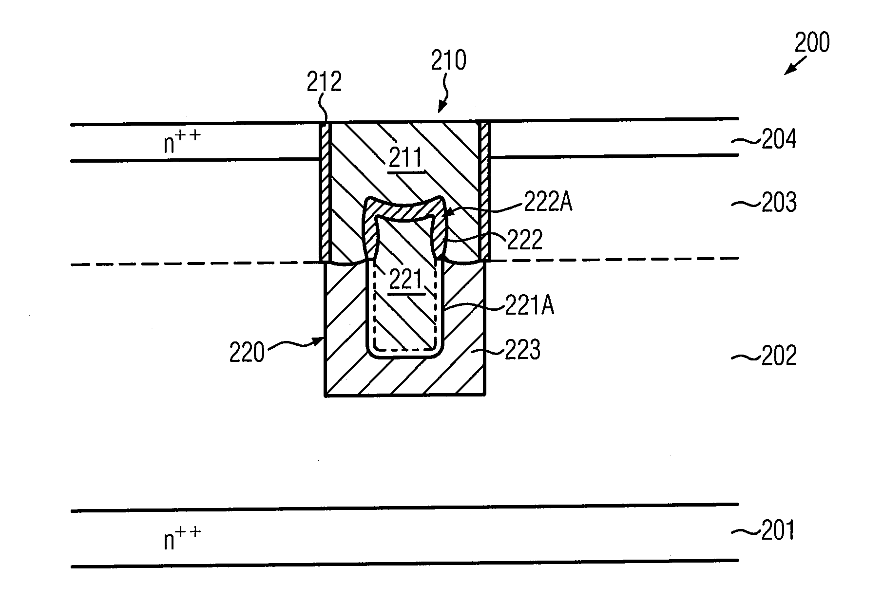
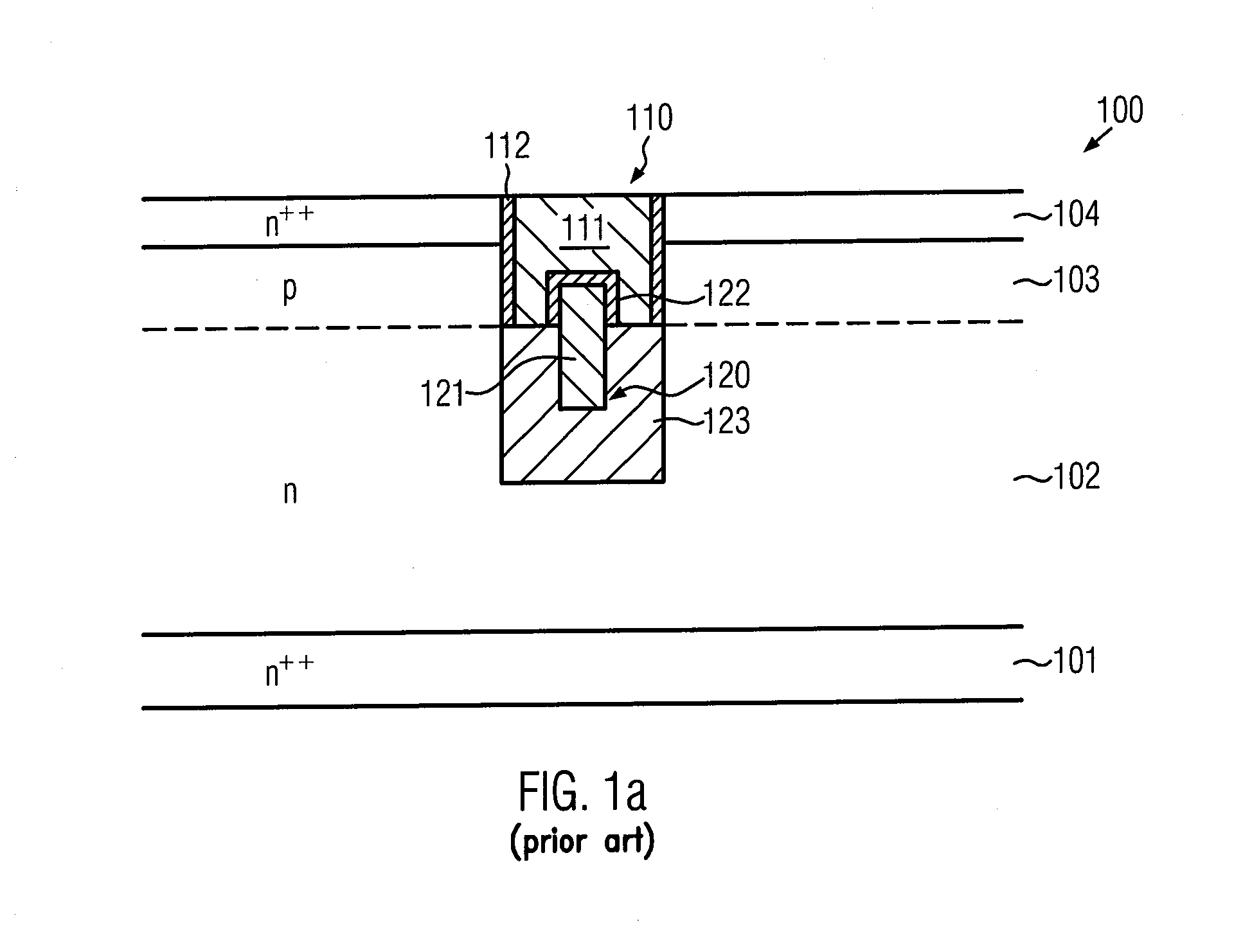
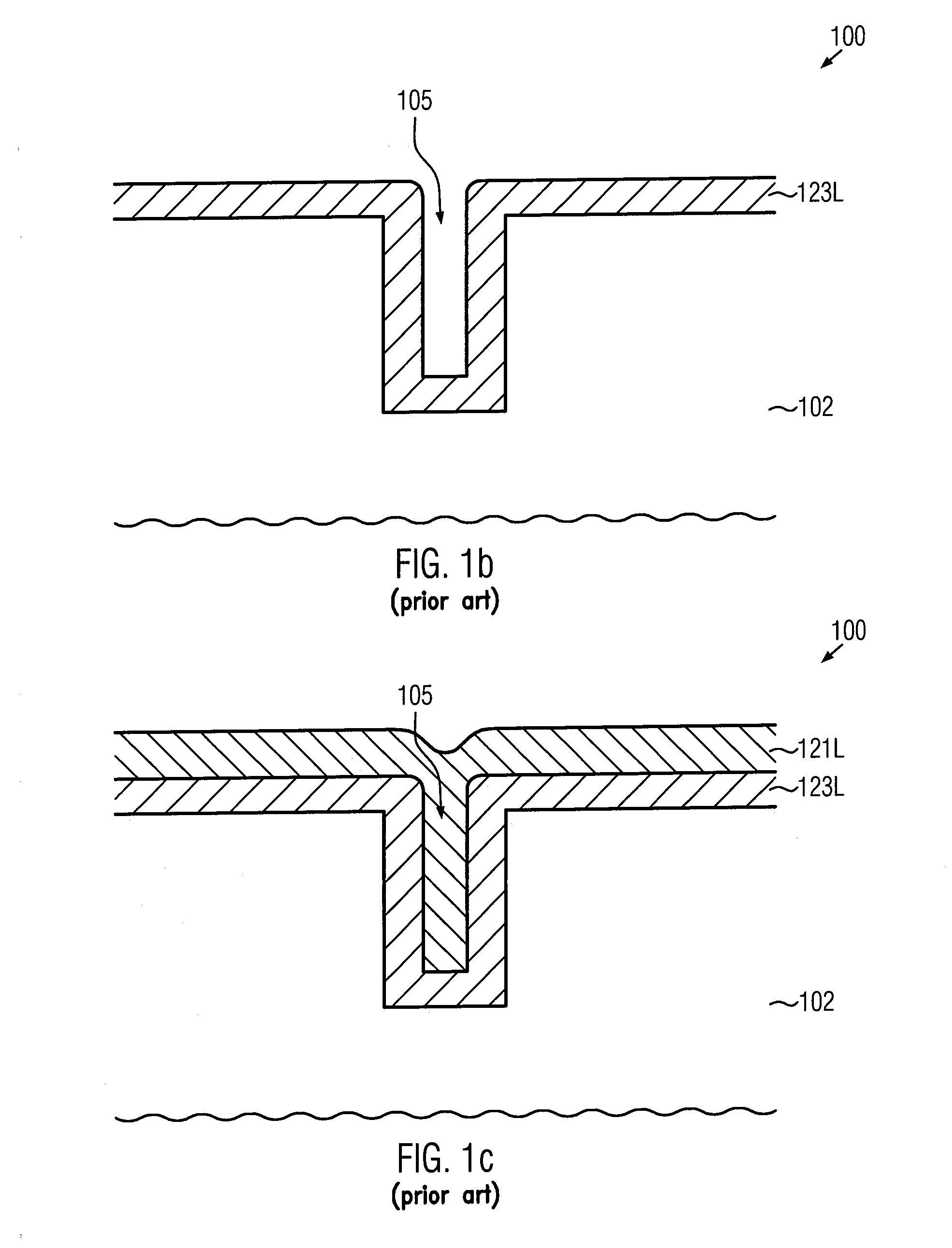
[0036]In one aspect of the present disclosure, a method is provided that relates to forming an MIS structure wherein the method comprises forming a first semiconductor electrode in a cavity that is formed in a crystalline semiconductor region, wherein the first semiconductor electrode is electrically insulated from the crystalline semiconductor region by an insulating layer. The method further comprises increasing an oxidation rate of at least a portion of a surface of the first semiconductor electrode relative to an exposed surface of the crystalline semiconductor region in the cavity. Additionally, the method comprises concurrently oxidizing the exposed surface of the crystalline semiconductor region in the cavity and an exposed surface of the first semiconductor electrode so as to form a first oxide layer on the exposed surface of the crystalline semiconductor region and a second oxide layer on the exposed surface of the first semiconductor electrode. Finally, the method comprise...


PUM


Abstract

In an MIS structure a field plate electrode is incorporated below a buried gate electrode by using an insulating oxide layer, which is formed concurrently with the gate dielectric layer. In order to obtain superior dynamic behavior and enhanced dielectric strength the oxidation behavior of the field plate electrode is modified, for instance by incorporating a desired high concentration of arsenic.

Description

BACKGROUND[0001]1. Technical Field[0002]The present disclosure generally relates to semiconductor devices including MIS (metal-insulator-semiconductor) structures formed using a “vertical” device architecture in which a current flow may be controlled by electric field more efficiently on the basis a “buried” field plate.[0003]2. Description of the Related Art[0004]In the field of semiconductor devices immense progress has been achieved by reducing the dimensions of the circuit elements and improving associated process techniques and process tools. The continuous shrinkage of critical feature sizes has, at one cutting edge of the semiconductor technology, resulted in the fabrication of extremely complex integrated circuits which may comprise millions of transistor elements, which may be operated using extremely low supply voltages. On the other hand, the advances in materials, process techniques and process tools have also fuelled the development of complex integrated circuits, which...

Claims


Application Information

Patent Timeline
Patent Type & Authority Applications(United States)
IPC IPC(8): H01L29/78H01L21/28
CPCH01L21/31658H01L21/32105H01L29/407H01L29/7813H01L29/42376H01L29/66734H01L29/42368H01L29/4236H01L29/7827
Inventor BORZI, ANNACOCCORESE, CORRADOMORALE, GIUSEPPEREPICI, DOMENICO
Owner STMICROELECTRONICS SRL
Why Eureka
Try Eureka