Semiconductor device

a semiconductor device and semiconductor technology, applied in the field of semiconductor devices, can solve the problems of increasing the number of wiring layers of the package substrate, obstructing the miniaturization and thinning of the semiconductor device, so as to achieve the effect of easy connection and increasing the contour size of the packag

Inactive Publication Date: 2006-08-17
RENESAS ELECTRONICS CORP
View PDF4 Cites 25 Cited by
  • Summary
  • Abstract
  • Description
  • Claims
  • Application Information

AI Technical Summary

Benefits of technology

[0003] With respect to the common signals and power source / ground in two chips which constitute the stacked package LSI, their pads are not always arranged to positions where they can be connected easily between the chips. Accordingly, even when the wiring layers are connected on the package substrate, in many cases, there exist crossing wiring layers or wiring layers are arranged densely. In these cases, the number of wiring layers of the package substrate is increased or a contour size is increased thus obstructing the miniaturization and thinning of the semiconductor device. Since connection terminals of mounting chips are formed individually, a large terminal arrangement area becomes necessary and this also becomes a cause of increasing the contour size of the package.
[0009] It is an object of the present invention to provide a semiconductor device having the stacked structure which can realize miniaturization and thinning of contour sizes.

Problems solved by technology

In these cases, the number of wiring layers of the package substrate is increased or a contour size is increased thus obstructing the miniaturization and thinning of the semiconductor device.
Since connection terminals of mounting chips are formed individually, a large terminal arrangement area becomes necessary and this also becomes a cause of increasing the contour size of the package.

Method used


Image

  • Semiconductor device
  • Semiconductor device
  • Semiconductor device

Examples


Embodiment Construction

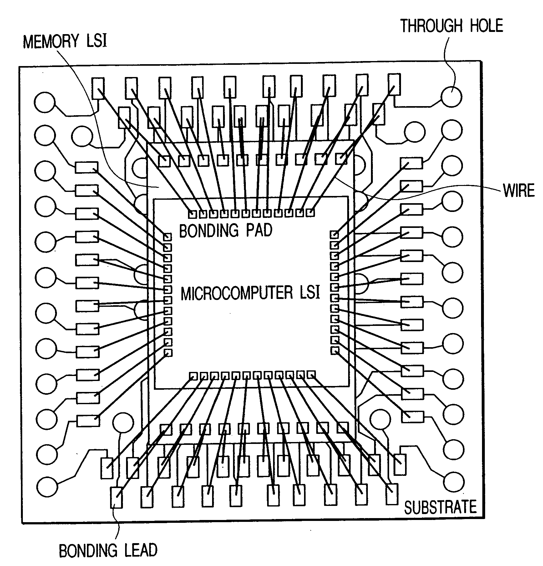
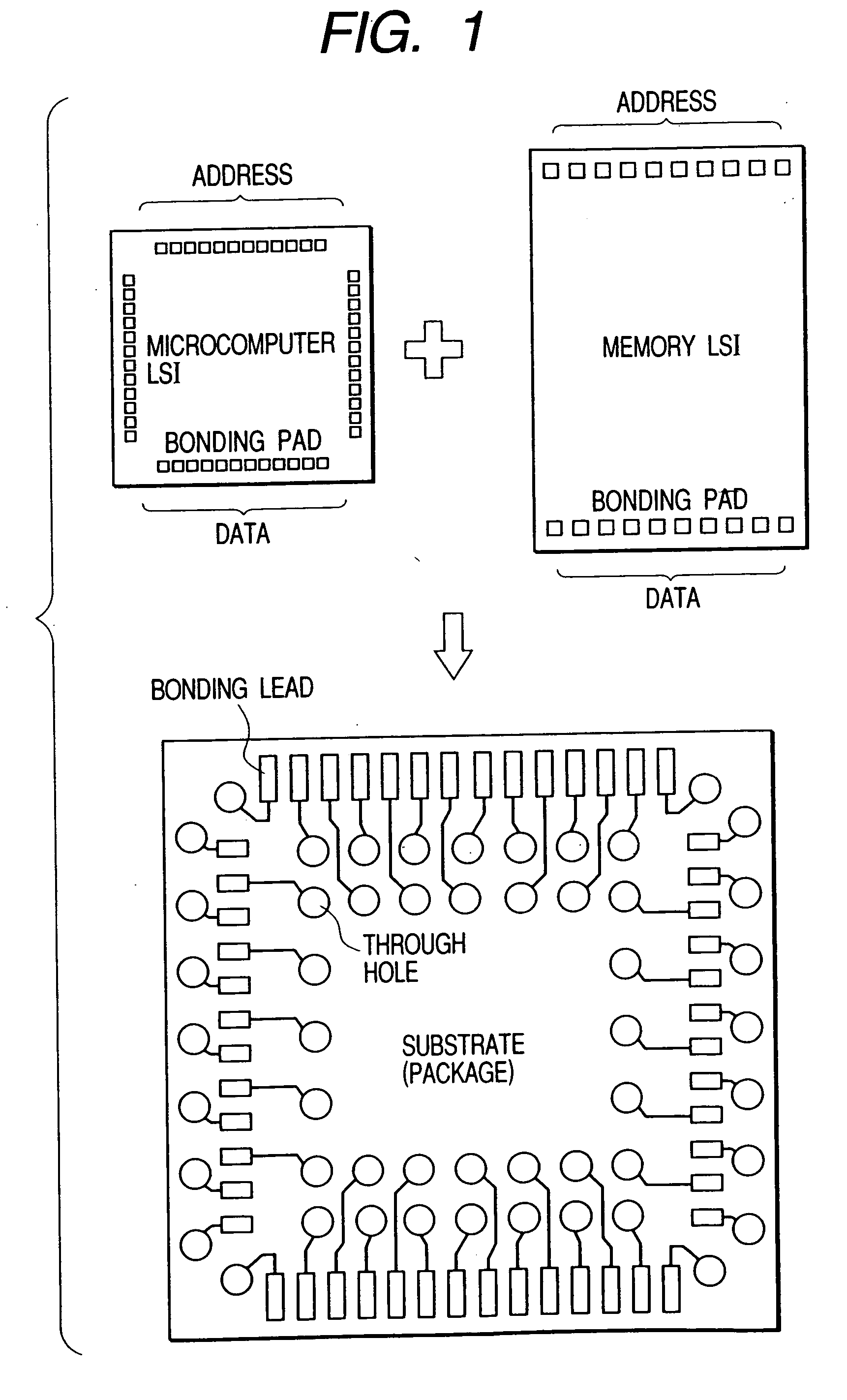
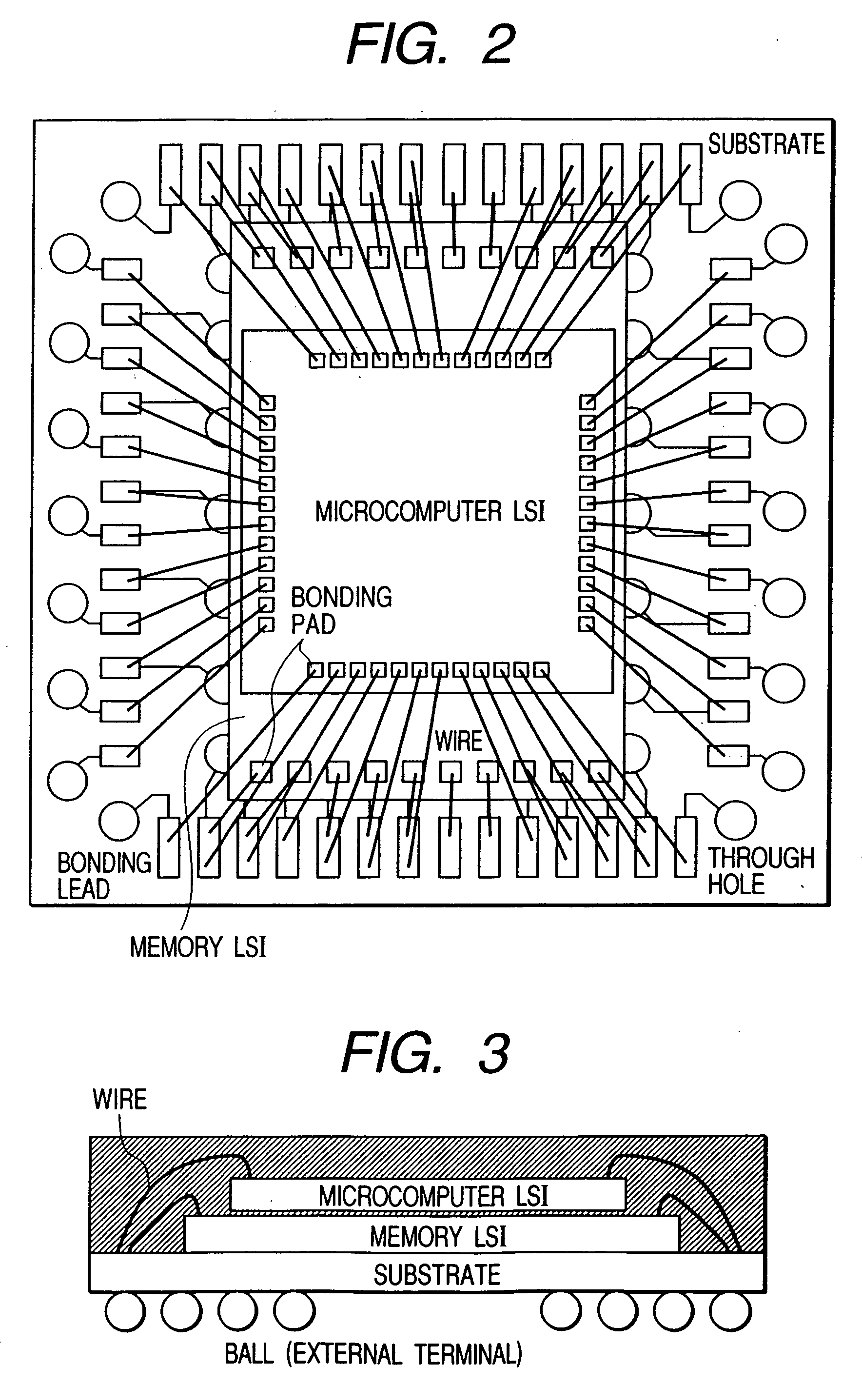
[0033] In FIG. 1 to FIG. 3, the constitution of one embodiment of a stacked package LSI according to the present invention is shown. That is, in FIG. 1, a microcomputer LSI, a memory LSI and a package substrate which constitute the stacked package LSI are respectively shown. In FIG. 2, an appearance of the stacked package LSI in a state that the memory LSI and the microcomputer LSI are mounted on the substrate and, thereafter, the wire bonding is performed is shown. FIG. 3 shows the cross section of the stacked package LSI. As shown in FIG. 1 to FIG. 3, the stacked package LSI of this embodiment has the structure which is formed as follows. That is, the memory LSI is die-bonded to the package substrate made of glass epoxy resin. Then, the microcomputer LSI is superposed on and is die-bonded to the memory LSI. Wire bonding is performed between the respective chips and the substrate. Thereafter, the respective chips and the substrate are molded with resin and solder balls are formed o...


PUM


Abstract

The present invention provides a semiconductor device having a stacked structure which realizes the miniaturization of a contour size and the reduction of thickness. The present invention also provides a semiconductor device which realizes high performance and high reliability in addition to the miniaturization of the contour size. The semiconductor device uses a package substrate on which bonding leads which are formed respectively corresponding to bonding pads for address and data which are distributed to opposing first and second sides of a memory chip and address terminals and data terminals which are connected to the bonding leads are formed. The semiconductor device further includes an address output circuit and a data input / output circuit which are also served for memory access and a signal processing circuit having a data processing function. A semiconductor chip in which bonding pads which are connected to the bonding leads corresponding to the address terminals of the package substrate and bonding pads which are connected to the bonding leads corresponding to the data terminals of the package substrate are distributed to two sides out of four sides and the above-mentioned memory chip are mounted on the package substrate in a stacked structure.

Description

BACKGROUND OF THE INVENTION [0001] The present invention relates to a semiconductor device, and more particularly to a technique which is effectively applicable to a semiconductor device in which a plurality of semiconductor chips are mounted on a package substrate in a laminated or stacked structure, for example. [0002] In a stacked LSI (Large-sized Integrated Circuit) which assembles semiconductor chips on a package substrate in a laminated or stacked structure, existing semiconductor chips are combined in many cases and common signals and power source / ground are connected via wiring layers of a package. Due to a prior art search which is carried out after the present invention was made, as a prior art related to the present invention, a technique disclosed in Japanese Unexamined Patent Publication 43531 / 2000 is reported. However the technique disclosed in this publication aims at the reduction of time and efforts necessary for designing and development of types of standard packag...

Claims


Application Information

Patent Timeline
Patent Type & Authority Applications(United States)
IPC IPC(8): H01L23/52H01L23/48H01L23/12H01L23/538H01L25/065H01L25/07H01L25/18
CPCH01L23/5386H01L25/0657H01L2924/15311H01L2924/1433H01L2924/14H01L2225/06555H01L25/18H01L2224/32145H01L2224/48091H01L2224/48227H01L2224/49171H01L2225/0651H01L2225/06527H01L2225/06541H01L2924/00014H01L2924/00H01L23/12
Inventor MIWA, TAKASHITSUTSUMI, YASUMIICHITANI, MASAHIROHASHIZUME, TAKANORISATO, MASAMICHIMORINO, NAOZUMINAKAMURA, ATSUSHITAMAKI, SANEAKIKUDO, IKUO
Owner RENESAS ELECTRONICS CORP
Why Eureka
Try Eureka