Plasma display panel

a technology of display panels and plasma, applied in the direction of static indicating devices, instruments, electrodes, etc., can solve the problems of discharge interference among adjacent cells, gaps between partitions, and surface of layers obtained by vapor deposition methods, so as to prevent discharge interference

Inactive Publication Date: 2006-08-24
HITACHI LTD
View PDF4 Cites 2 Cited by
  • Summary
  • Abstract
  • Description
  • Claims
  • Application Information

AI Technical Summary

Benefits of technology

[0011] The present invention is directed to solve the problem pointed out above, and therefore, an object of the present invention is to prevent discharge interference in plasma display panels in which partitions abut against an insulation layer on which projections are generated along display electrodes.
[0014] Preferably, the segment layers are made from materials that are the same as those of the row electrodes. The row electrodes and the segment layers are formed at the same time, followed by formation of the insulation layer, which eliminates the need for a specific step for providing the second projections. In the case where the row electrodes have a multilayered structure, the segment layers may have the same structure as that of the row electrodes or may have a structure in which the number of layers is smaller than the number of layers of the row electrodes. In either structure, the fact remains that a specific step is unnecessary to provide the second projections.
[0015] The present invention can prevent discharge interference in plasma display panels in which partitions abut against an insulation layer on which projections are generated along display electrodes.

Problems solved by technology

More specifically, surfaces of layers obtained by the vapor deposition method are not even unlike a surface of a low melting point glass layer that is burned at sufficiently high temperatures.
In plasma display panels including projections that are generated, along display electrodes, on an insulation layer for covering the display electrodes, a problem arises that gaps exist between partitions and parts other than the projections in the insulation layer and discharge interference is apt to occur among adjacent cells, compared to the case of plasma display panels having an insulation layer with a flat surface.

Method used


Image

  • Plasma display panel
  • Plasma display panel
  • Plasma display panel

Examples


Embodiment Construction

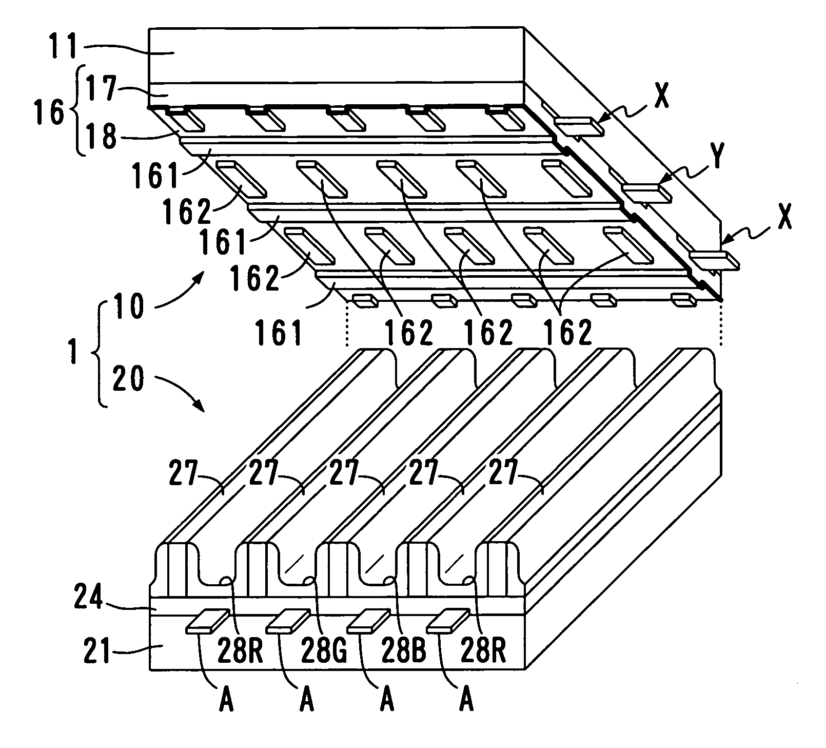
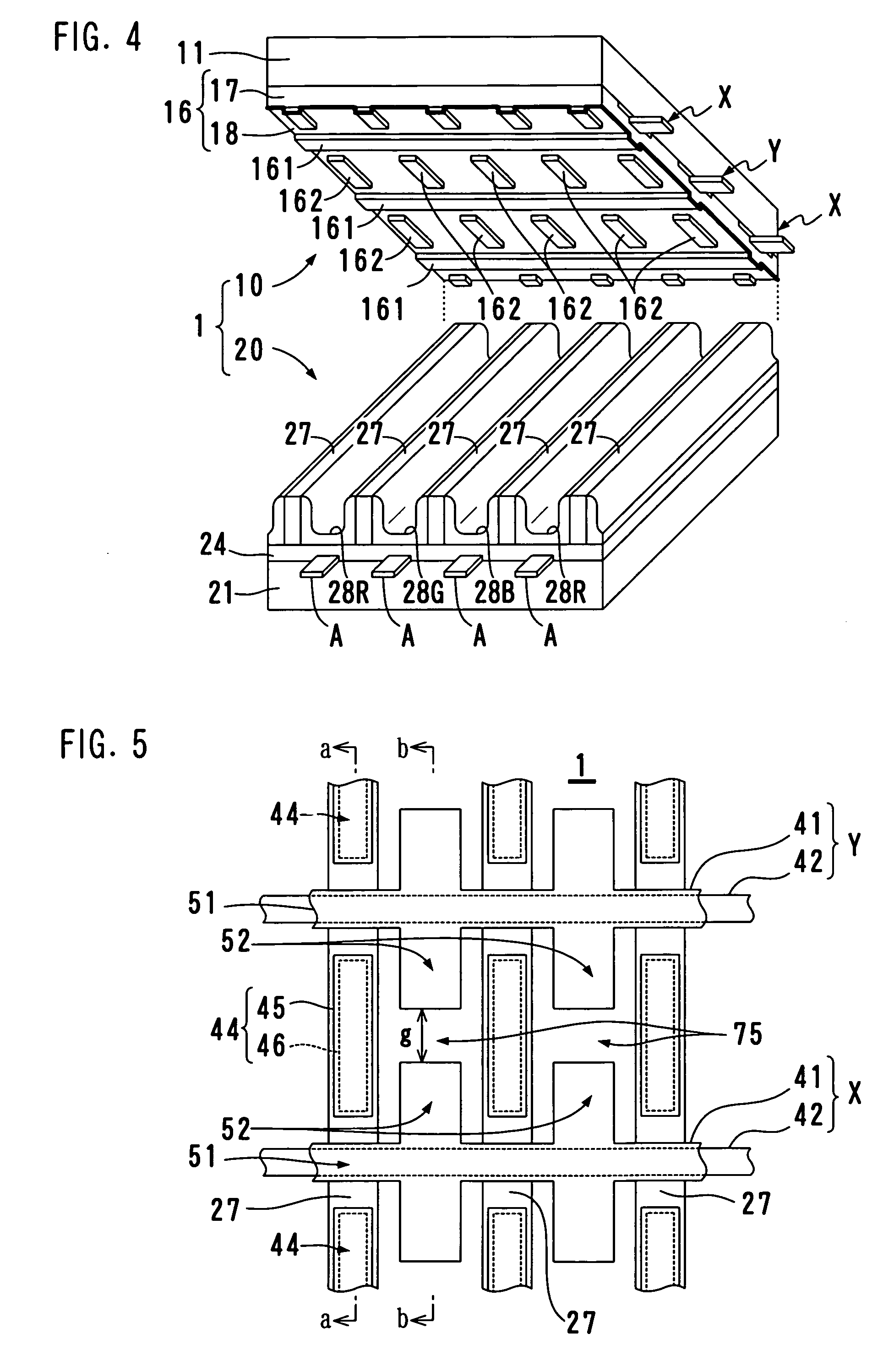
[0027] The present invention is suitably applied to plasma display panels for color display. The following is a description of a case of a three-electrode surface discharge AC type plasma display panel having a screen including many cells.

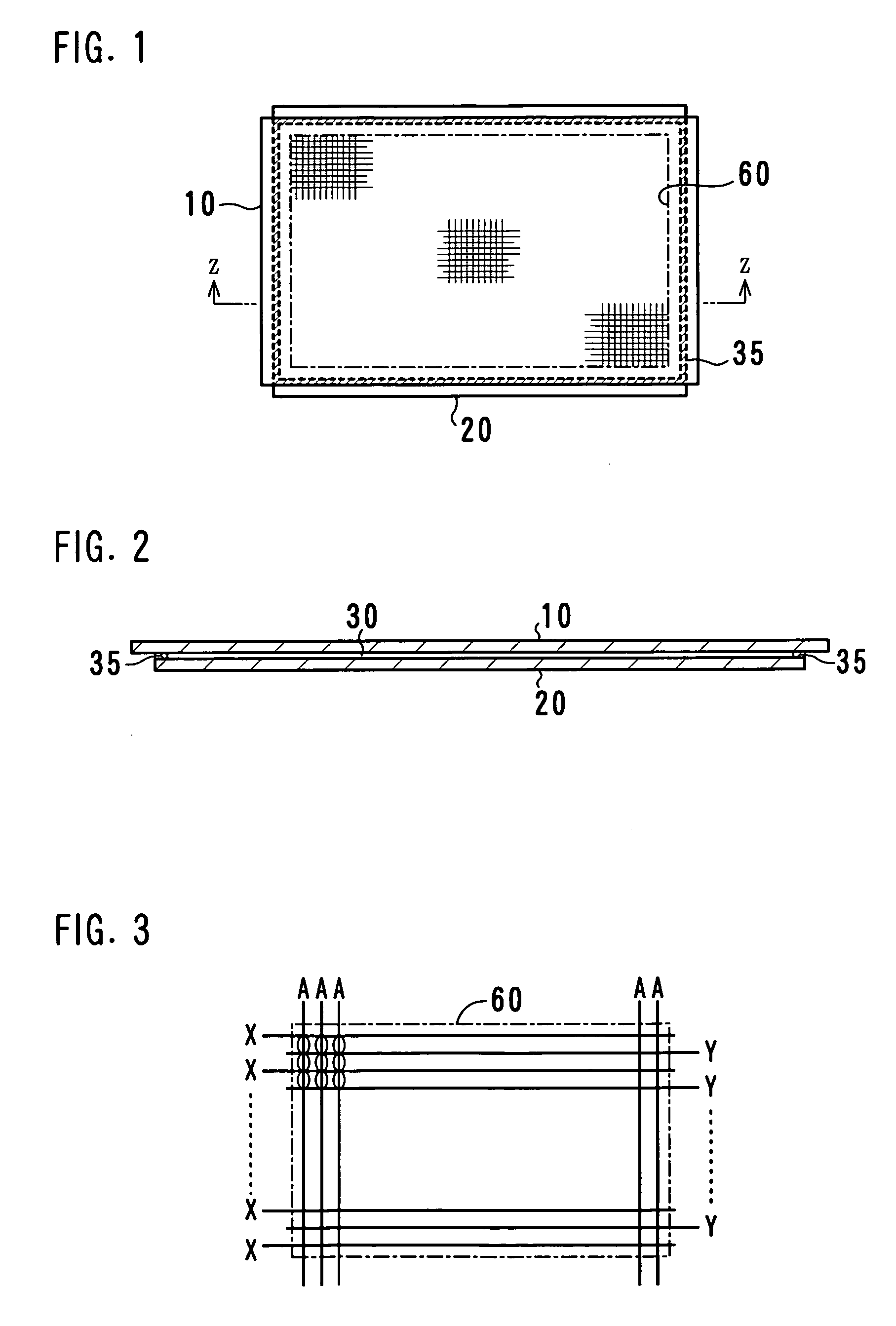
[0028] A basic structure of a plasma display panel is shown in FIGS. 1 and 2 respectively. FIG. 1 is a front view showing the entire structure of the plasma display panel, and FIG. 2 is a cross-sectional cut along z-z line in FIG. 1. The plasma display panel includes a front panel 10, a rear panel 20 and a screen 60 made up of cells (light emission elements) arranged in a matrix. In the case where the screen 60 is a 42-inch diagonal, for example, the plasma display has dimensions of approximately 994 mm×585 mm. Each of the front panel 10 and the rear panel 20 is a structure including a glass substrate on which electrodes and other structural elements are fixed. Both the glass substrates have a size larger than the screen 60 and a thickness of appr...


PUM


Abstract

A plasma display panel includes row electrodes arranged on a first substrate, an insulation layer for covering the row electrodes, partitions each of which is placed in a boundary between columns of the second substrate and is continuous over an entire length of the column and a first projection that is formed on a surface of the insulation layer and has a shape and a height corresponding to those of the row electrode. In such a plasma display panel, a segment layer covered with the insulation layer is positioned in a manner to overlap with the partition in the first substrate and to avoid overlap with the row electrode and a second projection is formed on the surface of the insulation layer. The second projection has a shape and a height corresponding to those of the segment layer and constitutes a part of a discharge barrier between the columns.

Description

BACKGROUND OF THE INVENTION [0001] 1. Field of the Invention [0002] The present invention relates to plasma display panels including projections that are generated, along electrodes, on a surface of an insulation layer for covering the electrodes. [0003] 2. Description of the Related Art [0004] An AC type plasma display panel includes a dielectric layer for covering display electrodes. The dielectric layer is formed on a substrate on which the display electrodes are arranged in a manner to extend over the entire screen. The dielectric layer that is made of low melting point glass, which is a general material, has a thickness of approximately 20 μm to 30 μm. A protection film is deposited on a surface of the dielectric layer. The protection film has a thickness of approximately 0.5 μm to 1 μm and serves to prevent sputtering due to discharges for the dielectric layer. Stated differently, the display electrodes are covered with a layered film including the dielectric layer and the pro...

Claims


Application Information

Patent Timeline
Patent Type & Authority Applications(United States)
IPC IPC(8): H01J17/49H01J11/12H01J11/22H01J11/24H01J11/26H01J11/30H01J11/32H01J11/34H01J11/38
CPCH01J11/12H01J11/36H01J11/38H01J11/32
Inventor SASAKI, TAKASHITAKAMORI, TAKAHIRO
Owner HITACHI LTD
Why Eureka
Try Eureka