Image forming apparatus

a technology charging roller, which is applied in the field of image forming apparatus, can solve the problems of image formation failure, low charging potential, and large nip distance difference between the charging roller and the photosensitive drum, and achieve the effect of preventing the occurrence of image formation failur

Active Publication Date: 2006-08-24
KYOCERA DOCUMENT SOLUTIONS INC
View PDF2 Cites 12 Cited by
  • Summary
  • Abstract
  • Description
  • Claims
  • Application Information

AI Technical Summary

Benefits of technology

[0009] In view of the above problems residing in the prior art, it is an object of the present invention to provide a contact charging type image forming apparatus equipped with a photoconductor, particularly, an amorphous silicon photosensitive drum, which is capable of substantially uniformly keeping a surface potential of the photoconductor in a direction of a rotational axis thereof, and to prevent occurrence of image formation failure such as fog.
[0011] With the above arrangement, the light guiding member for guiding the charge removing light is provided between the light source and the photoconductor, and the light guiding member is operative to control the amount of the charge removing light to be projected onto the surface of the photoconductor. This arrangement enables to control the charge removing light amount with use of the light guiding member, considering a nip distance difference between the photoconductor and the charger, a charge removing light amount fluctuation, and the like. Accordingly, this arrangement secures image formation without an image formation failure, while suppressing occurrence of a surface potential distribution non-uniformity of the photoconductor.

Problems solved by technology

This may lead to a lower charging potential on the axially central part, as compared with the axially opposite ends, which may cause a surface potential distribution non-uniformity of the photosensitive drum, and resultantly cause image formation failure such as fog.
In the case where an amorphous silicon photoconductor is used, a nip distance difference between the charging roller and the photosensitive drum greatly affects the surface potential distribution of the photosensitive drum.
Accordingly, the surface potential distribution non-uniformity cannot be sufficiently eliminated even by the approach of superimposing the AC bias voltage in the image forming apparatus provided with the amorphous silicon photosensitive drum.
Further, there is a case that a surface potential of a photosensitive drum may be fluctuated due to a charge removing light amount distribution non-uniformity.
If, however, the amount of the charge removing light is fluctuated axially, a charging fluctuation may occur, which may cause a surface potential distribution non-uniformity of the photosensitive drum, and resultantly lead to image formation failure such as fog.

Method used


Image

  • Image forming apparatus
  • Image forming apparatus
  • Image forming apparatus

Examples


first embodiment

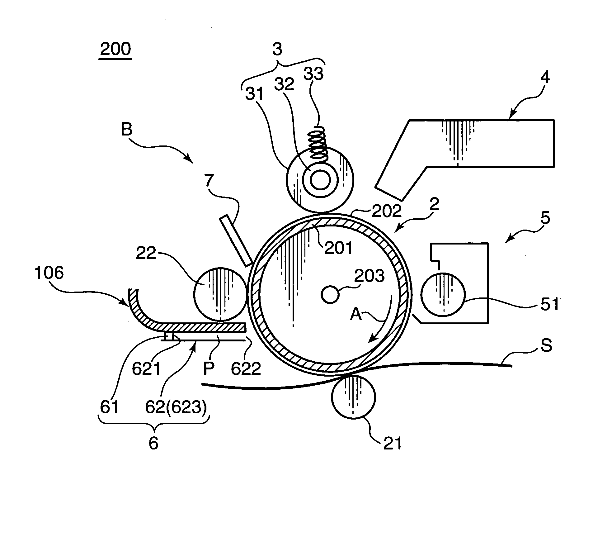
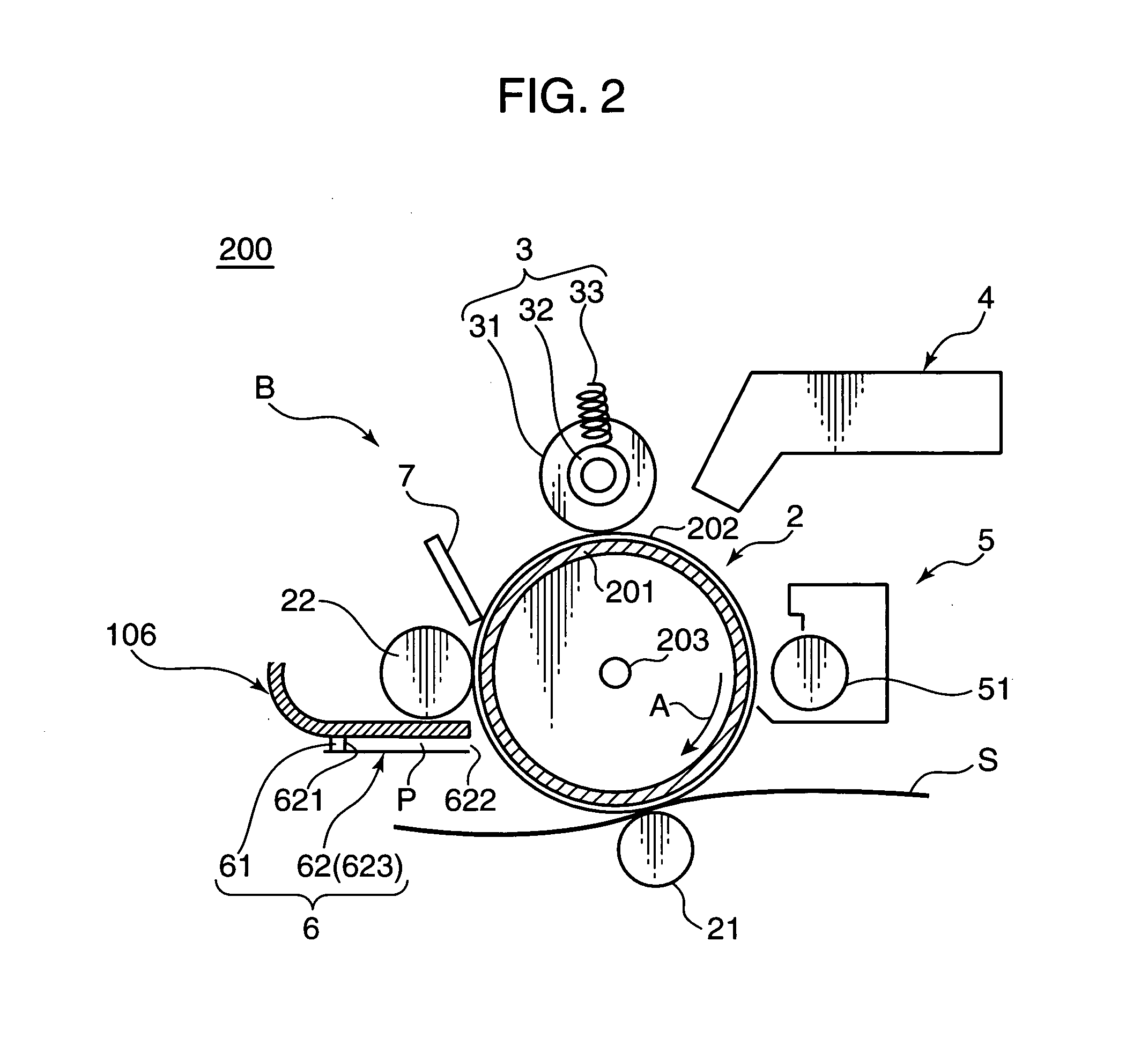
[0055] The above arrangement is employed in the first embodiment for the following reason. As shown in FIG. 4, in the image forming apparatus provided with the contact charging type charging roller 31 or the like, in order to bring the charging roller 31 into pressing contact with the photosensitive drum 2, it is required to provide the pressure springs 33 for urging the bearings 32 at the opposite ends of the charging roller 31 in view of likelihood that a sufficient pressing force may not be secured for the roller main body. Providing urging members such as the pressure springs 33, however, may result in a smaller load to be exerted to the axially central part of the photosensitive drum 2, as compared with the axially opposite ends thereof. As a result, the nip width between the photosensitive drum 2 and the charging roller 31 may be narrow on an axially central part C1, as compared with axially opposite ends C2. This may lower the surface potential i.e. the charging potential on ...

second embodiment

[0067] In the charge removing unit 6A in the second embodiment, a surface of a frame member 106, which is a component for defining a slit-like light transmitting space P of the light guiding member 62A, facing the light transmitting space P, has a substantially uniform reflectance to the charge removing light. On the other hand, a surface of an optical path defining member 623A facing the light transmitting space P has a locally varied reflectance to the charge removing light in order to vary the amount of the chare removing light to be projected onto the surface of the photosensitive drum 2 in the axial direction of the photosensitive drum 2.

[0068] As shown in FIG. 9, the optical path defining member 623A is produced by placing a first reflective member 6231 having a relatively low reflectance e.g. 50% or less in reflectance to the charge removing light, as a base member, and by attaching, on the base member, a second reflective member 6232 having a relatively high reflectance e.g....

third embodiment

[0084] The third embodiment is constructed as mentioned above for the following reason. As shown in FIGS. 3 and 11, in the case where the LED array 61 is used as a light source, wherein the LEDs 612, serving as point light sources, are arrayed in the axial direction of the photosensitive drum 2, the amount of the charge removing light to be projected along the second shortest lines L21, L22, . . . connecting the midpoints P1, P2, . . . of the adjacent LEDs 612 and the surface of the photosensitive drum 2 is made smaller than the amount of the charge removing light to be projected along the first shortest lines L11, L12, L13, . . . connecting the respective LEDs 612 and the surface of the photosensitive drum 2, because the second distance d4 is longer than the first distance d3. The lowering of the charge removing light amount is increased by increasing the interval between the respective LEDs 612. In other words, if the number of the LEDs 612 is decreased in order to reduce the prod...


PUM


Abstract

Charge removing light is guided by an optical path defining member (623) from a charge removing unit (6) toward a photosensitive drum (2). A distance between an end surface (623e) of the optical path defining member (623) and a surface on an axially central part of the photosensitive drum (2) is less than a distance between the end surface (623e) and the surface on the axially opposite ends of the photosensitive drum (2). Thus an irradiation width and an amount of the charge removing light projected onto the surface of the photosensitive drum (2) are increased on the opposite ends. With this arrangement, the amount of generated light carriers can be reduced on the axially central part, as compared with the axially opposite ends, and a surface potential distribution non-uniformity due to a difference in nip distance between the photosensitive drum (2) and a charging roller (31) can be eliminated.

Description

BACKGROUND OF THE INVENTION [0001] 1. Field of the Invention [0002] The present invention relates to an image forming apparatus provided with a photoconductor, particularly, an amorphous silicon (a-Si) photosensitive drum for charging a surface of the photosensitive drum by contact charging. [0003] 2. Description of the Related Art [0004] Heretofore, a device for electrostatically charging a drum-type electrophotographic photoconductor (hereinafter, simply called as “photosensitive drum”) has been composed of a corona charging device designed to expose a surface of a photosensitive drum to corona charge so as to electrostatically charge the surface. In recent years, from the aspect of advantages in lower-level ozone formation and lower power consumption as compared with the corona charging device, a contact charging type image forming apparatus, designed to bring a charging member such as a charging roller in a voltage-applied state into contact with a surface of a photosensitive dr...

Claims


Application Information

Patent Timeline
Patent Type & Authority Applications(United States)
IPC IPC(8): G03G21/06
CPCG03G21/08
Inventor TOMIIE, NORIOTOKUSHIGE, AKANE
Owner KYOCERA DOCUMENT SOLUTIONS INC
Why Eureka
Try Eureka