Semiconductor memory device with high operating current and method of manufacturing the same

a memory device and high operating current technology, applied in the direction of solid-state devices, water installations, soil shifting machines/dredgers, etc., can solve the problems of reducing the operating current failing to improve the operating current of both types of transistors of the semiconductor memory device, and reducing the mobility of the pmos transistor, so as to achieve the effect of increasing the mobility of both nmos transistor and pmos transistor, and forming self-aligning contact pads

Inactive Publication Date: 2006-08-24
SAMSUNG ELECTRONICS CO LTD
View PDF6 Cites 33 Cited by
  • Summary
  • Abstract
  • Description
  • Claims
  • Application Information

AI Technical Summary

Benefits of technology

[0009] The present invention provides a method of manufacturing a semiconductor memory device, which can increase the mobil

Problems solved by technology

However, a stress applying layer (etch stop layer) made of silicon nitride that induces tensile stress increases mobility of an N-channel metal oxide semiconductor (NMOS) transistor but decreases mobility of a P-channel metal oxide semiconductor (PMOS) transistor.
Accordingly, in a semiconductor memory device including both an NMOS transistor and the PMOS transistor, if the thickness of the etch stop layer made of silicon nitride is increased to improve the mobility of the

Method used


Image

  • Semiconductor memory device with high operating current and method of manufacturing the same
  • Semiconductor memory device with high operating current and method of manufacturing the same
  • Semiconductor memory device with high operating current and method of manufacturing the same

Examples


Embodiment Construction

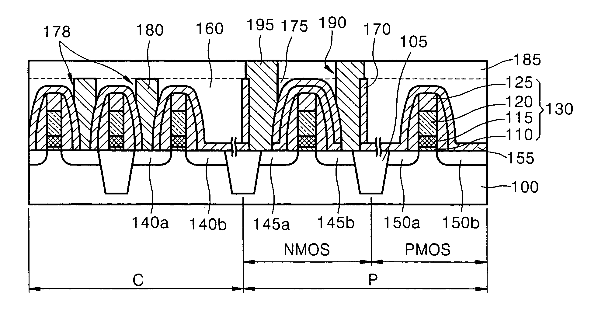
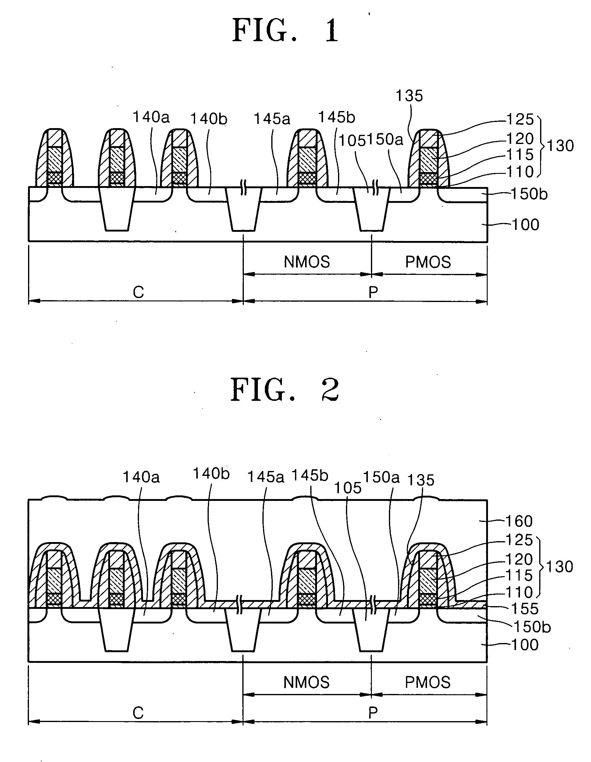
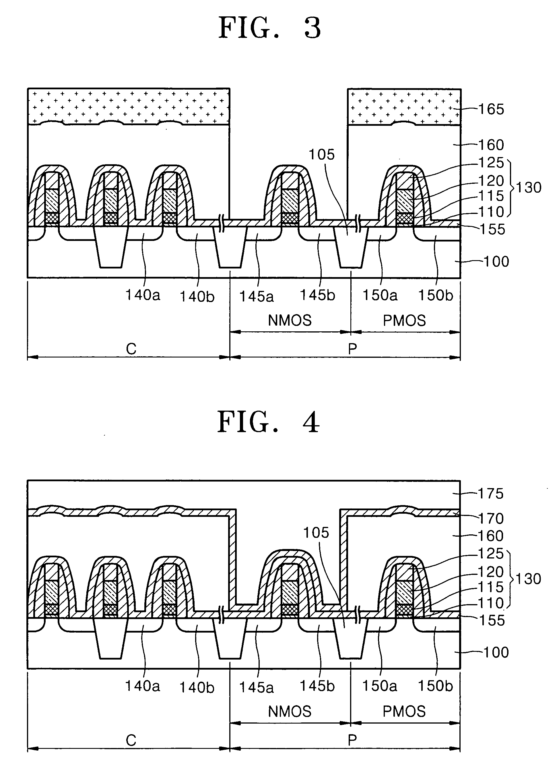
[0032] The present invention will now be described more fully hereinafter with reference to the accompanying drawings, in which preferred embodiments of the invention are shown. This invention may, however, be embodied in different forms and should not be construed as limited to the embodiments set forth herein. Like numbers refer to like elements throughout the specification. The shapes of elements in the drawings are exaggerated for the convenience of explanation.

[0033] According to a semiconductor memory device illustrated in the embodiments of the present invention, to increase the operating currents, that is, the mobilities, of both an N-type metal oxide semiconductor (NMOS) transistor and a P-type metal oxide semiconductor (PMOS) transistor in a common peripheral circuit region and easily form self-aligned contact pads in a memory cell region, an etch stop layer portion (referred to as an NMOS region hereinafter) where the NMOS transistor is formed is thicker than an etch sto...


PUM


Abstract

In a semiconductor memory device with a high operating current and a method of manufacturing the same, a semiconductor substrate is formed in which a memory cell region and a peripheral circuit region including an N-channel metal oxide semiconductor (NMOS) region and a P-channel metal oxide semiconductor (PMOS) region are defined. A gate electrode with sidewall spacers is formed in each of the memory cell region and the peripheral circuit region. Source and drain regions are formed in the semiconductor substrate at sides of the gate electrode to form metal oxide semiconductor (MOS) transistors. A first etch stop layer is formed on the semiconductor substrate where the MOS transistors are formed. A second etch stop layer is selectively formed in the NMOS region of the peripheral circuit region.

Description

BACKGROUND OF THE INVENTION [0001] This application claims the priority of Korean Patent Application No. 10-2005-0014091, filed on Feb. 21, 2005, in the Korean Intellectual Property Office, the disclosure of which is incorporated herein in its entirety by reference. FIELD OF THE INVENTION [0002] The present invention relates to a semiconductor memory device and a method of manufacturing the same, and more particularly, to a semiconductor memory device with a high operating current and a method of manufacturing the same. DESCRIPTION OF THE RELATED ART [0003] It is well known that the performance of a transistor largely depends on an operating current of the transistor. Accordingly, methods to obtain high operating current in transistors are continuously being studied. One such approach is referred to as strained silicon channel (SSC) technology, in which stress is applied to a channel region. [0004] SCC technology provides a strained channel layer by forming a stress-applying layer o...

Claims


Application Information

Patent Timeline
IPC IPC(8): H01L21/84H01L21/31
CPCH01L21/76801H01L21/76831H01L21/76832H01L21/76897H01L21/823871H01L27/105H01L27/11526H01L27/11546H01L29/6656H01L29/7843H01L27/1052H10B99/00H10B41/40H10B41/49E02B5/08E03F5/14E02F5/28
Inventor KIM, WOOK-JE
Owner SAMSUNG ELECTRONICS CO LTD
Why Eureka
Try Eureka