Methods for semiconductor passivation by nitridation

a technology of nitridation and semiconductor, applied in the direction of semiconductor devices, semiconductor/solid-state device details, electrical devices, etc., to achieve the effect of high mobility

Active Publication Date: 2016-12-08
ASM IP HLDG BV
View PDF3 Cites 315 Cited by
  • Summary
  • Abstract
  • Description
  • Claims
  • Application Information

AI Technical Summary

Benefits of technology

[0007]In some embodiments, a method for integrated circuit fabrication is provided. The method comprises passivating the surface of a substrate comprising a high mobility semiconductor by removing native semiconductor oxide from the surface; subsequently forming a semiconductor oxide-containing film on the surface; and thermally nitriding the semiconductor oxide-containing film by exposing the semiconductor oxide-containing film to at least one of hydrazine and a hydrazine derivative.

Problems solved by technology

However, the passivation of high mobility semiconductors faces various challenges and work continues on developing suitable passivation techniques for these materials.

Method used


Image

  • Methods for semiconductor passivation by nitridation
  • Methods for semiconductor passivation by nitridation
  • Methods for semiconductor passivation by nitridation

Examples


example 1

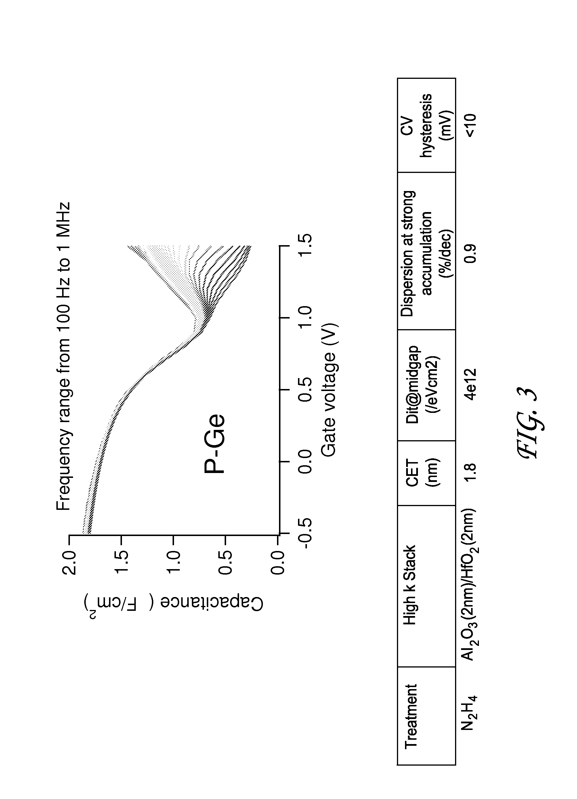
[0045]Hydrazine passivation of germanium was investigated in a metal oxide semiconductor (MOS) capacitor, which has a structure similar to a MOS transistor, except that PN junctions (and source / drain regions) are absent. The germanium was part of a 1.5 μm germanium layer grown epitaxially on a silicon wafer and p-doped. The substrate was then pre-treated by being dipped in HF. The pre-treated p-doped germanium-containing substrate surface was then passivated by exposure to hydrazine in a Pulsar® ALD reactor available from ASM International N.V. of Almere, the Netherlands. The exposure duration was 1 minute, at a process temperature of 250° C. A 2 nm aluminum oxide layer and then a 2 nm hafnium oxide layer were deposited to form a dielectric stack over and contacting the hydrazine-treated surface. Platinum was deposited on the dielectric stack as a gate electrode, thereby forming the MOS capacitor. The platinum was deposited by evaporation, which included depositing platinum dots on ...

example 2

[0048]Passivation of p-doped and n-doped germanium using a germanium oxynitride layer was investigated in a MOS capacitor. As in Example 1, the germanium was part of a 1.5 μm germanium layer grown epitaxially on a silicon wafer and p-doped and n-doped. The substrate was then pre-treated by being dipped in HF. A germanium oxynitride layer was deposited on each of a p-doped and n-doped germanium substrate. The deposition was performed a Pulsar® ALD reactor available from ASM International N.V. of Almere, the Netherlands. The germanium oxynitride interlayer as deposited by ALD using tetrakis(dimethylamino)germanium (TDMAGe) as the germanium precursor, H2O as the oxygen precursor, and hydrazine (N2H4) as the nitrogen precursor. Each deposition cycle included the following sequence of pulses:

[0049]TDMAGe

[0050]H2O

[0051]TDMAGe

[0052]N2H4

[0053]Ten cycles were performed, with N2H4 exposure durations of a few second each time. The durations of the precursor pulses and intervening purges were,...


PUM


Abstract

In some embodiments, a semiconductor surface having a high mobility semiconductor may be effectively passivated by nitridation, preferably using hydrazine, a hydrazine derivative, or a combination thereof. The surface may be the semiconductor surface of a transistor channel region. In some embodiments, a semiconductor surface oxide layer is formed at the semiconductor surface and the passivation is accomplished by forming a semiconductor oxynitride layer at the surface, with the nitridation contributing nitrogen to the surface oxide to form the oxynitride layer. The semiconductor oxide layer may be deposited by atomic layer deposition (ALD) and the nitridation may also be conducted as part of the ALD.

Description

[0001]BACKGROUND[0002]Field[0003]This disclosure relates generally to semiconductor processing and, more particularly, to passivation of semiconductor substrates, including passivation of channel regions of transistors.[0004]Description of the Related Art[0005]Semiconductor materials that exhibit high charge-carrier mobility have gained interest as possible materials for use in various electronic devices, such as transistors in integrated circuits. High charge-carrier mobility materials have a higher charge-carrier mobility than silicon, and may improve the performance of these electronic devices, relative to forming the devices using silicon as the only semiconductor. Examples of high charge-carrier mobility semiconductor materials include silicon germanium, germanium and group III-V semiconductor materials, such as GaAs, InP, InGaAs, InAs, and GaSb.[0006]The passivation of semiconductor materials can improve the electrical properties of devices formed with these materials, and may...

Claims


Application Information

Patent Timeline
Patent Type & Authority Applications(United States)
IPC IPC(8): H01L21/02H01L29/10H01L29/20H01L23/31H01L29/16
CPCH01L21/02247H01L23/3171H01L21/02255H01L21/02249H01L29/1033H01L29/16H01L29/20H01L21/02301H01L21/02205H01L21/0228H01L21/02112H01L21/2807H01L29/518
Inventor XIE, QITANG, FUGIVENS, MICHAELRAISANEN, PETRIMAES, JAN WILLEM
Owner ASM IP HLDG BV
Why Eureka
Try Eureka