Highly-sensitive displacement-measuring optical device

a displacement measurement and optical device technology, applied in the field of measurement devices, can solve the problems of nonlinear detection scheme, micro-machined capacitive microphones of today, use of high impedance amplifiers, etc., and achieve the effects of high resolution and precision, slow imaging, and general improvement of lateral resolution of interferometers

Inactive Publication Date: 2006-08-31
GEORGIA TECH RES CORP
View PDF82 Cites 79 Cited by
  • Summary
  • Abstract
  • Description
  • Claims
  • Application Information

AI Technical Summary

Problems solved by technology

There are various drawbacks to today's micromachined capacitive microphones.
These attributes are, in fact, in conflict, as the maximum DC bias that can be used is limited by the electrostatic collapse voltage, which decreases with shrinking gap height.
Unfortunately, the detection scheme becomes nonlinear under this same condition.
In addition to this drawback, implementation of the constant charge condition can require the use of high impedance amplifiers, which come with high electronic noise.
Even this approach is limited, however, by membrane stresses that result during fabrication.
These stresses bound the mechanical sensitivity that can be achieved and make the fabrication of uniform membranes with high yield difficult.
The perforation reduces the active capacitance and adversely affects Se, leading to yet another design conflict.
In summary, the electrical and mechanical sensitivity in a micromachined capacitive microphone are not independent and impose severe design and fabrication limitations.
Unfortunately, the size of the interferometer becomes rather large and subsequently may not fit in small spaces for inspection.
Furthermore, to inspect a large number of microscale structures either the sample or microscope objective is scanned, resulting in slow imaging.

Method used


Image

  • Highly-sensitive displacement-measuring optical device
  • Highly-sensitive displacement-measuring optical device
  • Highly-sensitive displacement-measuring optical device

Examples


Embodiment Construction

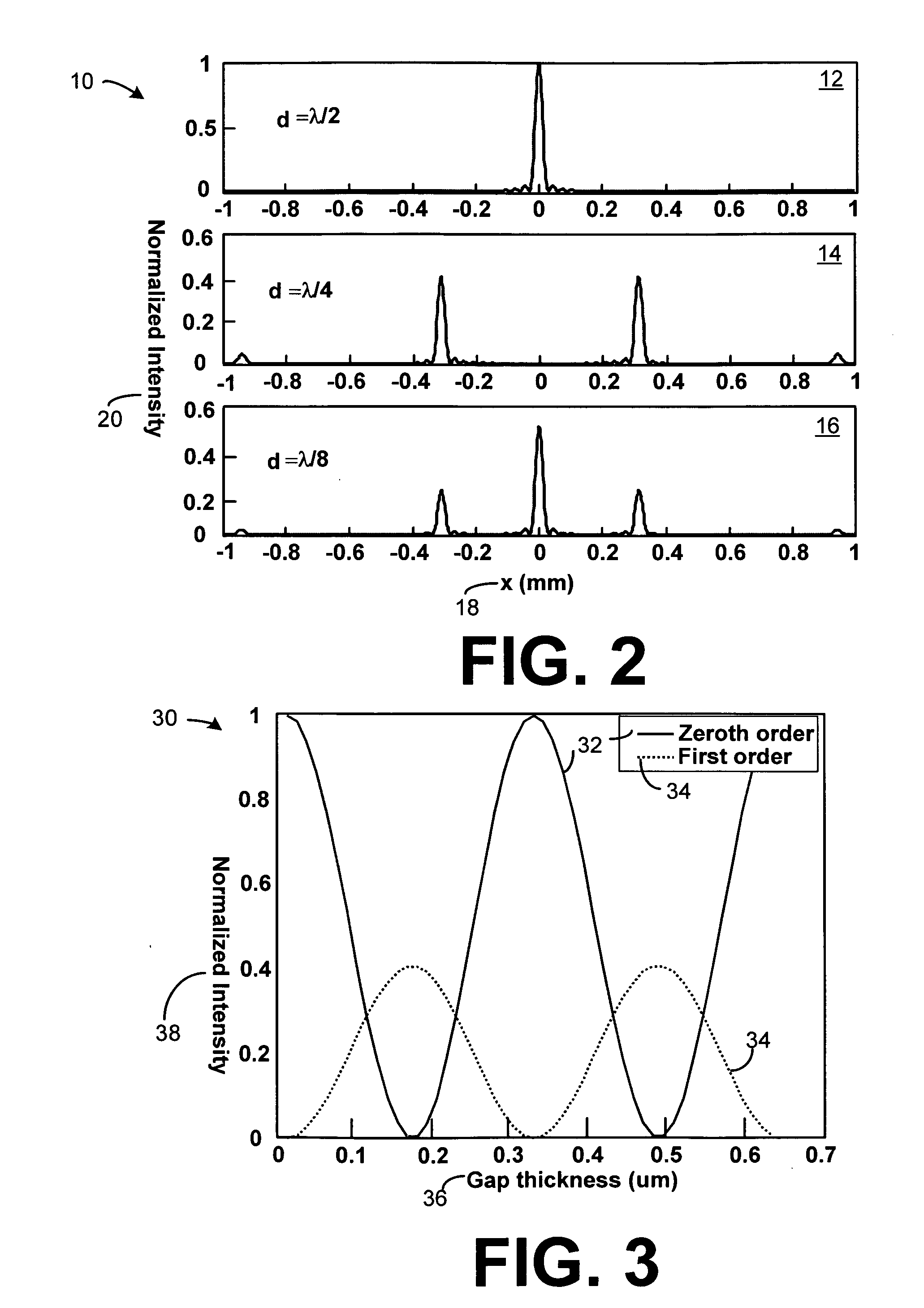
[0029] As will be described in greater detail herein, displacement measurement devices in accordance with the present disclosure can measure the change in position of a membrane as a function of time due to a variety of factors. Furthermore, the displacement measurement devices can be optimized for displacement sensitivity and reduced noise causing a greater signal to noise ratio (SNR).

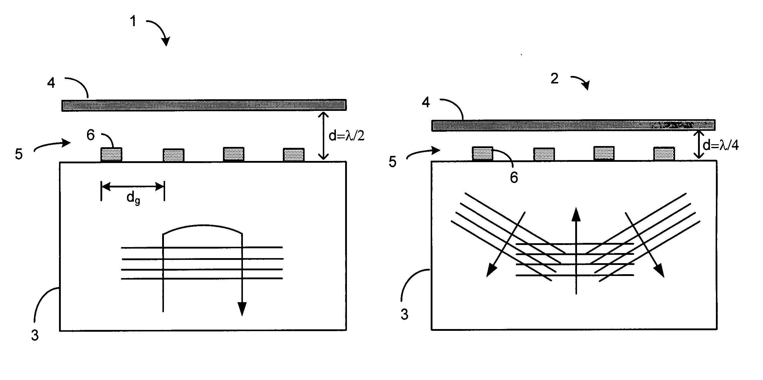
[0030] Referring now in more detail to the drawings, FIG. 1 is a diagram illustrating the concept of using a diffraction grating to split beams in a microinterferometer. This concept has been utilized in measuring precise relative displacements, such as for the measurement of Atomic Force Microscopy (AFM) tip displacement and in spatial light modulators, as in the grating light valves (GLV). This concept is also disclosed in U.S. Pat. No. 6,567,572 entitled“Optical Displacement Sensor” to F. L. Degertekin, G. G. Yaralioglu, and B. Khuri-Yakub, which is incorporated by reference in its entirety. AFM, ...


PUM


Abstract

Micron-scale displacement measurement devices having enhanced performance characteristics are disclosed. One embodiment of a micron-scale displacement measurement device includes a phase-sensitive reflective diffraction grating for reflecting a first portion of an incident light and transmitting a second portion of the incident light such that the second portion of the incident light is diffracted. The device can further include a mechanical structure having a first region and a second region, the mechanical structure positioned a distance d above the diffraction grating and forming a wall of a cavity, the second portion of the incident light is reflected off of the first region of the structure such that an interference pattern is formed by the reflected first portion and the reflected second portion of the incident light. The device can further include an orifice formed in the cavity to provide for the passage of air between the inside and outside of the cavity.

Description

CROSS-REFERENCE TO RELATED APPLICATIONS [0001] This application is a Continuation-in-Part application of co-pending U.S. utility patent application “Highly-Sensitive Displacement-Measuring Optical Device,” having Ser. No. 10 / 704,932, filed Nov. 10, 2003, which claims priority to U.S. provisional application “Miniature Diffraction-Based Optical Sensors,” having Ser. No. 60 / 424,810 filed Nov. 8, 2002, and to which claims priority to, and is a Continuation-in-Part of, “Microinterferometers With Performance Optimization,” having Ser. No. 10 / 112,490, filed Mar. 29, 2002 (now U.S. Pat. No. 6,753,969), each of which are incorporated by reference in their entirety. [0002] This application is also related to co-pending U.S. utility patent application entitled “System and Method for Surface Profiling,” having Ser. No. 10 / 113,362, filed Mar. 29, 2002. [0003] This application is related to co-pending commonly assigned Non-Provisional application entitled, “System and Method for Surface Profilin...

Claims


Application Information

Patent Timeline
Patent Type & Authority Applications(United States)
IPC IPC(8): G01B11/02G01B9/02
CPCG01D5/266H04R23/008G01B11/026G01B9/02051G01B2290/30
Inventor HALL, NEAL ALLENDEGERTEKIN, FAHRETTIN LEVENT
Owner GEORGIA TECH RES CORP
Why Eureka
Try Eureka