Light emitting element mounting member, and semiconductor device using the same

Active Publication Date: 2006-09-07
SUMITOMO ELECTRIC IND LTD
View PDF12 Cites 93 Cited by
  • Summary
  • Abstract
  • Description
  • Claims
  • Application Information

AI Technical Summary

Benefits of technology

[0015] It would be preferable for an electrode to be disposed on the main surface side of the semiconductor light-emitting element and electrically connected to the first and/or the second conductor region. In this case, since the electrode is disposed on the main surface side and the electrode is directly connected electrically to the first and/or the second conductor region, the heat generated by the light-emission layer, whi

Problems solved by technology

When a ceramic having aluminum oxide as its main component (hereinafter referred to also as alumina) is used in the substrate and the window frame, adequate heat dissipation is not possible, leading to increased temperature.
Furthermore, if aluminum nitride, which has high thermal con

Method used


Image

  • Light emitting element mounting member, and semiconductor device using the same
  • Light emitting element mounting member, and semiconductor device using the same
  • Light emitting element mounting member, and semiconductor device using the same

Examples


first embodiment

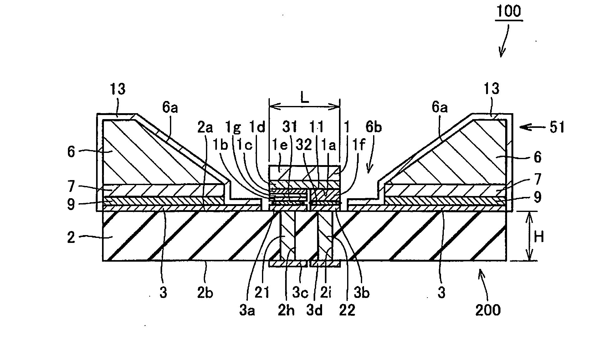
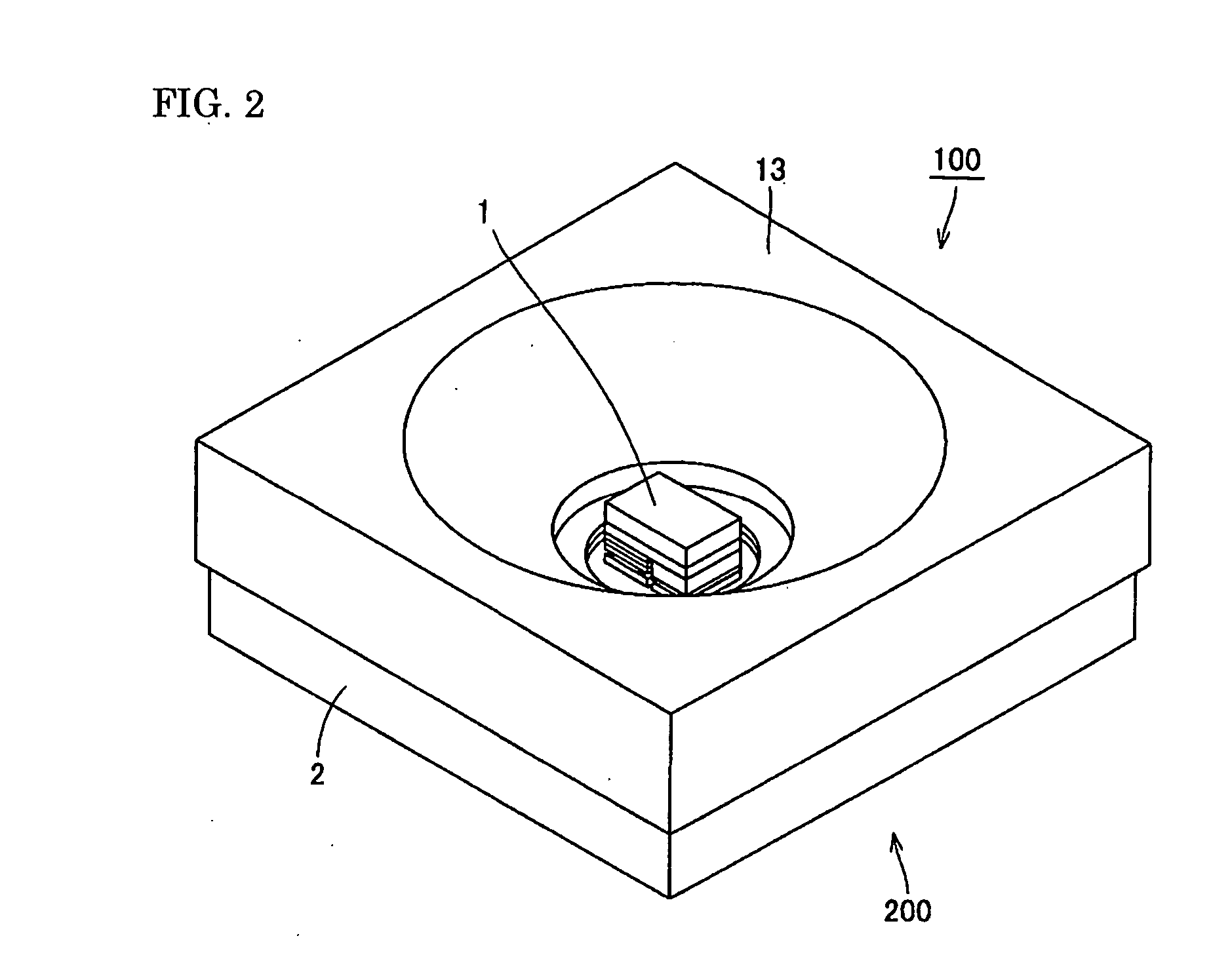
[0030]FIG. 1 is a cross-section drawing of a light-emitting element mounting member according to a first embodiment of the present invention and a semiconductor device using the same. FIG. 1A is a cross-section drawing of a semiconductor device according to one aspect. FIG. 1B is a cross-section drawing of a semiconductor device according to another aspect. FIG. 2 is a perspective drawing of the semiconductor device shown in FIG. 1A. FIG. 3 is a perspective drawing of the semiconductor light-emitting element shown in FIG. 1A. As shown in FIG. 1A, FIG. 2, and FIG. 3, a semiconductor device 100 according to the first embodiment of the present invention includes: a light-emitting element mounting member 200; and a semiconductor light-emitting element 1 mounted on an element mounting surface 2a. The semiconductor light-emitting element 1 includes a main surface 1a facing the element mounting surface 2a. In this example, the main surface 1a is formed as a rectangle including a longer fir...

second embodiment

[0068]FIG. 13 is a cross-section drawing of a light-emitting element mounting member and a semiconductor device that uses the same according to a second embodiment of the present invention. As shown in FIG. 13, in the light-emitting element mounting member 200 according to the second embodiment of the present invention, metal films 4, 4a, 4b are formed on the element mounting surface 2a, and the metal films 4, 4a, 4b are formed from Ag or Al. In this case, as shown in FIG. 13, it is possible to have the metal layer 13 formed only on the reflective member 6.

[0069] In this case, the same advantages are provided as those of the light-emitting element mounting member 200 and the semiconductor device 100 according to the first embodiment.

working example

[0070] A detailed study into the characteristics of the bonding layer 9 bonding the substrate 2 and the reflective member 6 was performed using a working example. Referring to FIG. 1, the reflective member 6 was attached to the element mounting surface 2a of the substrate 2 formed from aluminum nitride, interposed by the bonding layer 9. The reflective member 6 is an Ni—Co—Fe alloy with an Ni proportion of 29% by mass, a Co proportion of 18% by mass, and an Fe proportion of 53% by mass. Also, the dimensions of the reflective member 6 were set to 5 mm×5 mm×1 mm (height×width×thickness).

[0071] For the bonding layer 9, the sample 1 through the sample 8 from Table 1 were used.

TABLE 1ElectrodemetallizedpatternSampleMaterial for theBondingHeatHeatdegradationNo.bonding layer 9temperatureresistance 1resistance 2Strength(Au film 3)Notes1SolderAu—Ge 12%360° C.◯◯◯◯⊚2Ag—Cu 28%780° C.◯◯◯XDiscoloration in Au immediatelyafter bonding; Film thicknessreduced3Au—Sn 20%280° C.XX◯◯Re-melting of bond...


PUM


Abstract

The object of the present invention is to provide a light-emitting element mounting member and a semiconductor device using the same that is easy to process and that allows adequate heat dissipation.
A light-emitting element mounting member 200 includes: a substrate 2 including an element mounting surface 2a mounting a semiconductor light-emitting element 1 and first and second conductive regions 21, 22 disposed on the element mounting surface 2a and connected to the semiconductor light-emitting element 1; a reflective member 6 including a reflective surface 6a defining an internal space 6b for housing the semiconductor light-emitting element 1 and containing a metal disposed on the element mounting surface 1a; and a metal layer 13 disposed on the reflective surface 6a. The reflective surface 6a is sloped relative to the element mounting surface 2a so that a diameter of the internal space 6b is greater away from the element mounting surface 2a.

Description

TECHNICAL FIELD [0001] The present invention relates to a light-emitting element mounting member and a semiconductor device using the same. More specifically, the present invention relates to a light-emitting mounting element for mounting a light-emitting diode, a semiconductor laser, or the like and a semiconductor device using the same. BACKGROUND ART [0002] An example of a conventional member for mounting semiconductor light-emitting elements is described in Japanese Laid-Open Patent Publication Number 2002-232017. [0003] In the semiconductor mounting member described in this publication, a substrate and a ceramic window frame surrounding a light-emitting element is formed from a ceramic having as its main component aluminum oxide, aluminum nitride, or the like. [0004] With the increase in output in light-emitting elements in recent years, there has also been an increase in heat generated by semiconductor light-emitting elements. When a ceramic having aluminum oxide as its main c...

Claims


Application Information

Patent Timeline
IPC IPC(8): F21V7/04H01J1/62H01L33/00H01L33/60H01L33/62H01L33/64H01S5/00H01S5/02H01S5/022
CPCH01L33/486H01L33/60H01S5/0224H01S5/02292H01L2224/48091H01L2224/48465H01L2224/73265H01L2924/00014H01L2224/16225H01L2924/00H01L2224/05573H01L2224/05568H01L2224/05644H01L2224/06102H01L2224/1703H01L24/05H01S5/0234H01S5/02255
Inventor ISHIDU, SADAMUHIGAKI, KENJIROISHII, TAKASHITSUZUKI, YASUSHI
Owner SUMITOMO ELECTRIC IND LTD
Why Eureka
Try Eureka