Chromeless phase shifting mask for integrated circuits

a phase shifter and integrated circuit technology, applied in the field of photolithographic processing techniques, can solve the problems of difficult to create masks that use phase shifters for the smallest components and other exposure techniques for larger features, and difficult to print the smallest features of the latest circuit design with chrome patterns

Active Publication Date: 2006-09-07
SIEMENS PROD LIFECYCLE MANAGEMENT SOFTWARE INC
View PDF55 Cites 48 Cited by
  • Summary
  • Abstract
  • Description
  • Claims
  • Application Information

AI Technical Summary

Benefits of technology

This patent describes a way to make patterns on wafers by using a special kind of light called an extreme ultraviolet (EUV) laser. A computer program controls how this light interacts with a layer of material on the surface of the wafer to form different shapes like lines, holes, and other objects. These patterns help improve the performance of semiconductors, which are important components of many electronic devices.

Problems solved by technology

This patent discusses a problem in traditional photolithographic processing where it becomes harder to print smaller features due to limitations related to printing with chrome patterns. To solve this issue, researchers developed a method called phase shifting, which uses special masks to create desirable patterns on semiconductor devices. However, current methods make it challenging to create masks for all sizes of features and may struggle to produce high quality results. Thus, the technical problem addressed in this patent is how to develop a tool that allows for easy conversion from design layout to mask features while ensuring optimal performance across various size ranges.

Method used


Image

  • Chromeless phase shifting mask for integrated circuits
  • Chromeless phase shifting mask for integrated circuits
  • Chromeless phase shifting mask for integrated circuits

Examples


Embodiment Construction

[0019] As indicated above, the present invention is a method for decomposing a layout of features to be created in an integrated circuit design into mask pattern data used to create corresponding photolithographic masks that will in turn create the circuit features on a wafer.

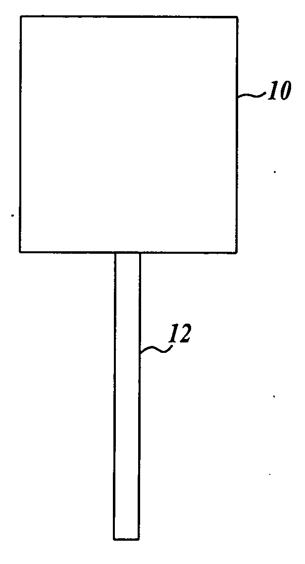
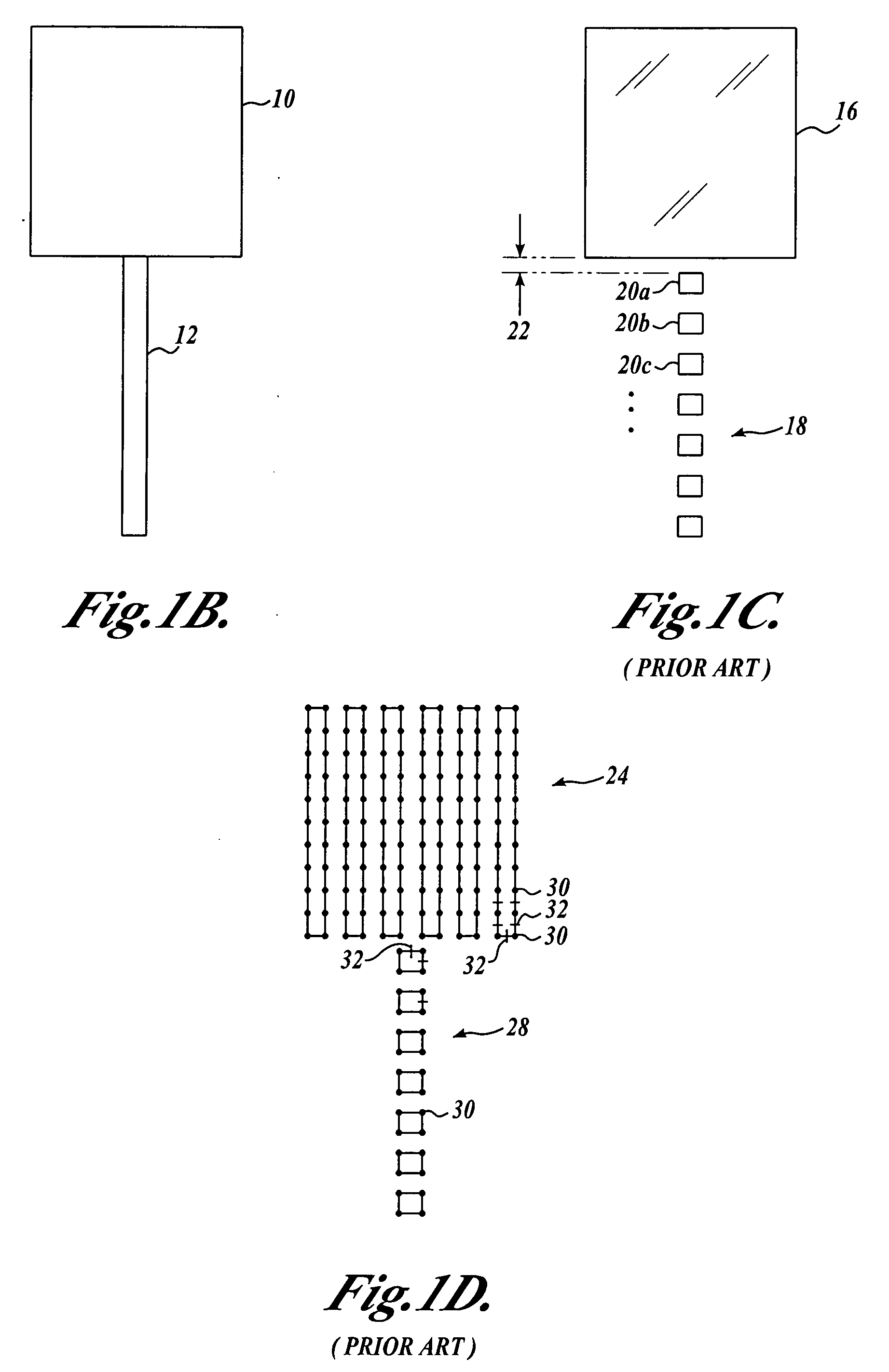
[0020]FIG. 1B illustrates a simplified pattern of features in a layout that are to be created on a semiconductor wafer. The pattern includes a large square area 10 which may represent a contact pad that is joined to a thinner feature 12, which may represent a transistor gate. The contact pad 10 may be large enough that it can be created using a conventional chrome-on-glass pattern on a photolithographic mask. However, the thinner feature 12 is too small to be created with a conventional chrome pattern and therefore must be made by some other technique such as by using a phase shifter. In order to avoid having to create the pattern of features on a wafer with a double exposure process and two masks, so called “...


PUM


Abstract

A system for creating mask layout pattern data in order to create a number of desired features on a semiconductor wafer. Critical features and features that are adjacent to or abut critical features are formed as phase shifting regions on a mask. Larger, non-critical features can be formed as annular rim shifters and may include one or more filling phase shifting regions. Non-critical features that are not adjacent to critical features and/or sub-resolution features that are not desired to print on the wafer can be formed as opaque or partially transparent regions on the mask.

Description


Claims


Application Information

Patent Timeline
Owner SIEMENS PROD LIFECYCLE MANAGEMENT SOFTWARE INC
Why Eureka
Try Eureka