CAD system for a printed circuit board

Inactive Publication Date: 2006-09-07
ORION ELECTRIC CO LTD
View PDF8 Cites 18 Cited by
  • Summary
  • Abstract
  • Description
  • Claims
  • Application Information

AI Technical Summary

Benefits of technology

[0019] According to the third aspect of the present invention, in the CAD system for a printed circuit board of the second aspect, there is provided a CAD system for a printed circuit board, wherein the judgment mark formed by combining Gerber data in accordance with proper procedures is formed in a shape common to each of the films. Therefore, if the shapes of judgment marks to be formed are different dependi

Problems solved by technology

Thus, in the case where a plurality of types of Gerber data are incorrectly combined with each other by an erroneous operation during that process, of course, the film finally produced is different from an expected pattern.
Conventionally, however, even if one item of Gerber data is mistakenly combined due to such an incorrect operation, it is impossible

Method used


Image

  • CAD system for a printed circuit board
  • CAD system for a printed circuit board
  • CAD system for a printed circuit board

Examples


Embodiment Construction

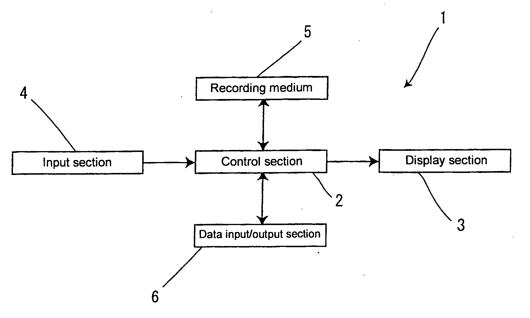
[0033] Hereinafter, an embodiment which is the best mode for carrying out the present invention will be described with reference to FIGS. 1 to 13. The following embodiment is provided as a mere aspect for embodying the present invention, and is not provided to limit the present invention within the scope of the embodiment.

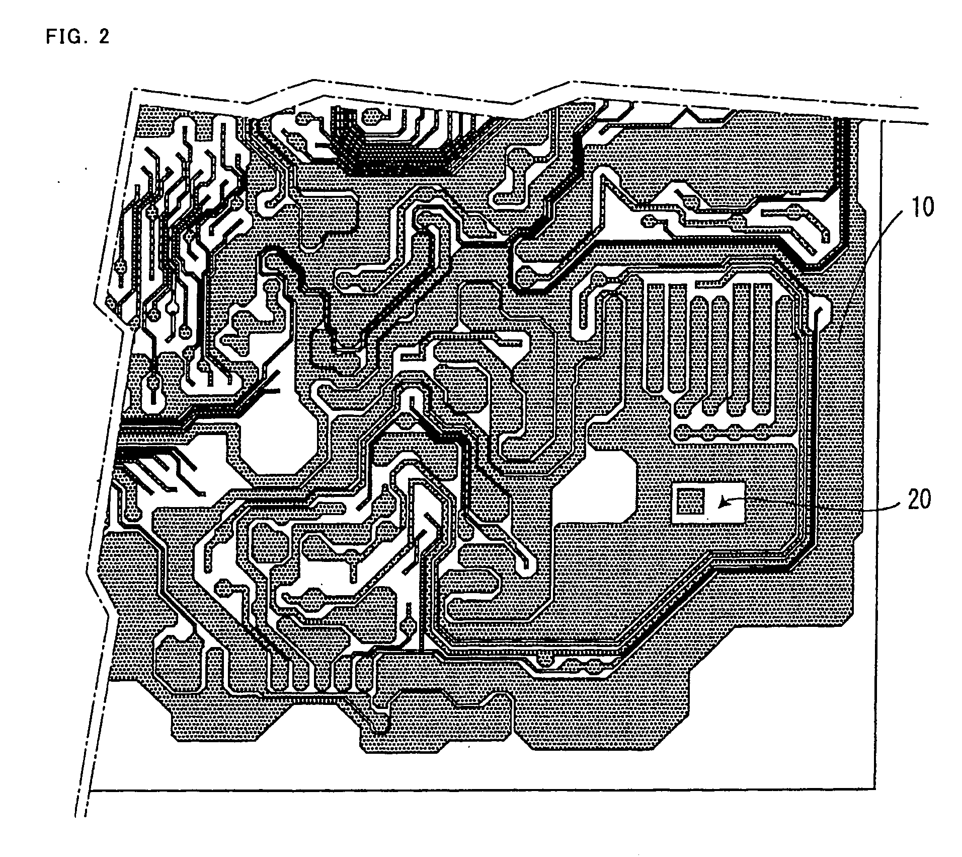
[0034]FIG. 1 is a block diagram schematically depicting a CAD system; FIG. 2 is a front view showing pattern Gerber data; FIG. 3 is a front view showing pattern cut Gerber data; FIG. 4 is a front view showing a pattern film; FIG. 5 is a front view showing resist Gerber data; FIG. 6 is a front view showing resist cut Gerber data; FIG. 7 is a front view showing a resist film; FIG. 8 is a front view showing silk Gerber data; FIG. 9 is a front view showing forced silk Gerber data; FIG. 10 is a front view showing a silk film; and FIGS. 11 to 13 show judgment marks of each film, wherein FIG. 11(a) shows a judgment mark of the pattern film when Gerber data is combined pr...


PUM


Abstract

A pattern design of a film for manufacturing a printed circuit board is made by using a CAD system, and a plurality of types of Gerber data are produced in which a series of various data has been encoded. For example, a pattern film is formed by combining pattern Gerber data with pattern cut Gerber data. Data for check marks whose sizes are different from each other is added as well as pattern data to each Gerber data such that their central coordinates are to be the same. In this manner, a judgment mark having the check marks combined therewith is formed on the pattern film having the items of Gerber data combined therewith.

Description

BACKGROUND OF THE INVENTION [0001] 1. Field of the Invention [0002] The present invention relates to a CAD system for a printed circuit board for producing a plurality of types of Gerber data, hierarchically combining these items of Gerber data, and designing film data for manufacturing a printed circuit board. In particular, the present invention relates to a CAD system for a printed circuit board capable of precisely making judgment whether a film is properly produced within a short period of time. [0003] 2. Description of the Related Art [0004] Conventionally, there has been known a manufacturing technique using a film negatively printed to fabricate a printed circuit board on which electric devices or the like, for example, are to be mounted. Now, the most general manufacturing technique will be described below. First, a film in which a wiring pattern has been negatively printed is laminated on a photosensitive substrate of which a copper foil coated with a resist (photosensitiv...

Claims


Application Information

Patent Timeline
IPC IPC(8): G06F17/50G06G7/62
CPCG06F17/5068H05K1/0269H05K3/0002H05K3/0005H05K3/0082H05K3/064H05K2201/09918H05K2203/056G06F30/39
Inventor ISHIMOTO, TOSHIOOKAYAMA, NAOFUMISASAKI, TOSHIHIKO
Owner ORION ELECTRIC CO LTD
Why Eureka
Try Eureka