Control circuit and control method
- Summary
- Abstract
- Description
- Claims
- Application Information
AI Technical Summary
Benefits of technology
Problems solved by technology
Method used
Image

Examples
embodiment 1
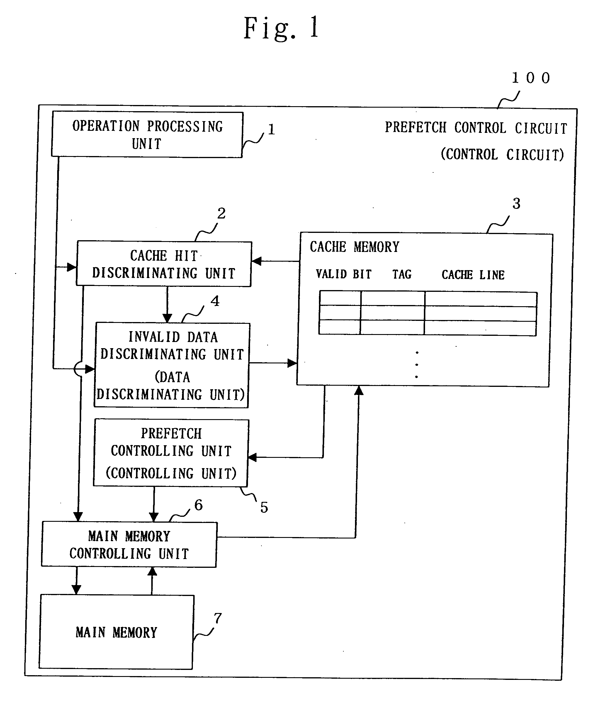
[0029]FIG. 1 shows a block diagram of a prefetch control circuit 100 according to the first embodiment.
[0030] In FIG. 1, a reference numeral 1 shows an operation processing unit which accesses a cache memory 3, reads data from the cache memory 3, and performs an operation on the read data.
[0031]2 shows a cache hit discriminating unit which discriminates whether a target data exists in the cache memory 3 or not at accessing time to the cache memory 3.
[0032]3 is a cache memory which stores data by a cache line unit.
[0033]4 is an invalid data discriminating unit which invalidates a cache line stored in the cache memory 3 based on the access to the cache memory 3.
[0034]5 shows a prefetch controlling unit which, when a valid cache line and an invalid cache line exist in the cache memory 3, obtains an original address of the target data for prefetch from an address of the valid cache line, and reads the target data for prefetch from a main memory 7 to store in the cache memory 3.
[00...
embodiment 2
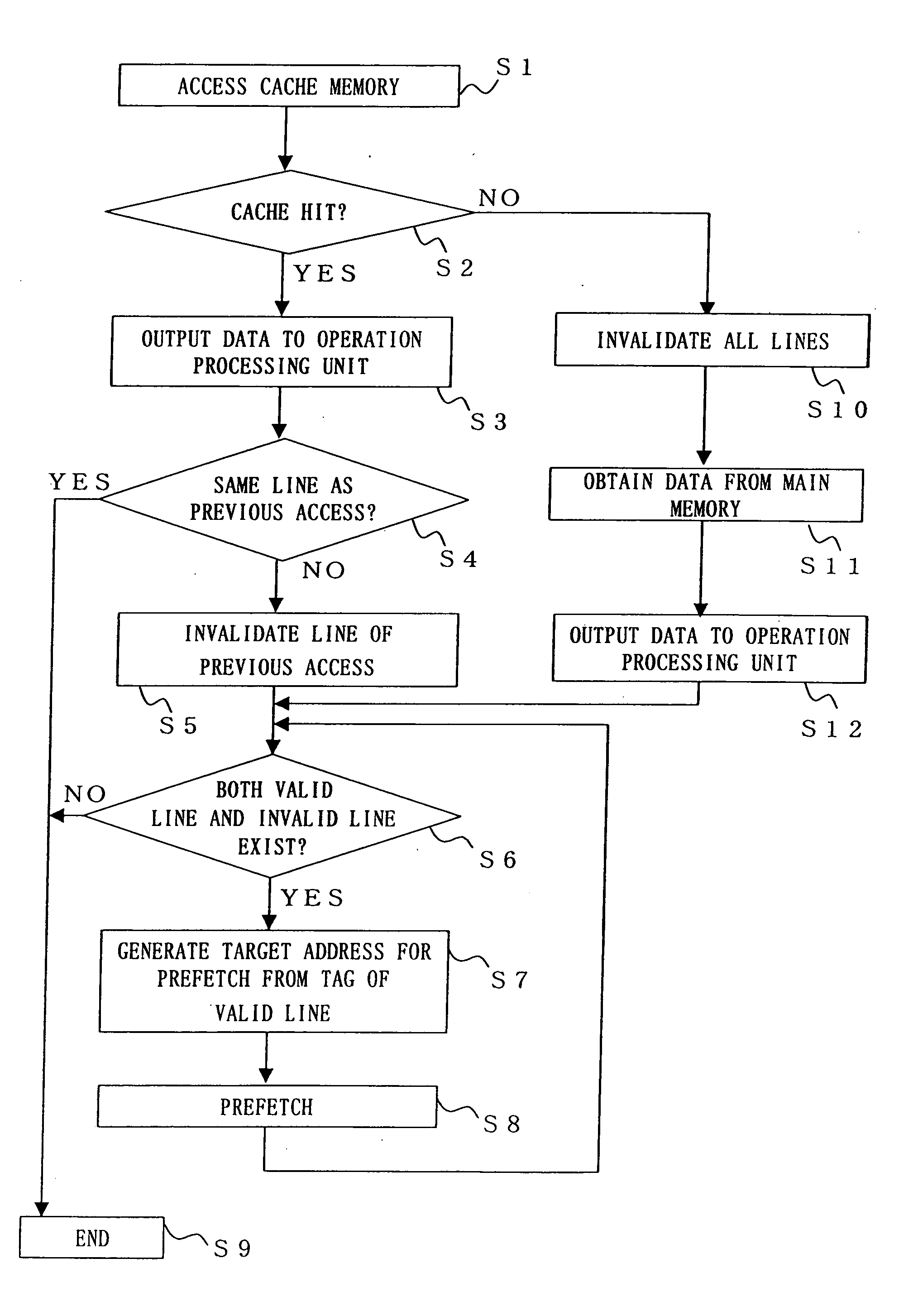
[0065] In the above first embodiment, the operation has been explained in which the operation processing unit 1 prefetches the data when the operation processing unit 1 accesses the cache memory 3 and a cache hit occurs.
[0066] In the second embodiment, another prefetching operation will be explained in reference to FIG. 2 when the operation processing unit 1 accesses the cache memory 3 and a cache miss occurs.
[0067] Similarly to the first embodiment, in FIG. 2, the operation processing unit 1 accesses the cache memory 3 (step S1), and the cache hit discriminating unit 2 discriminates whether the target data accessed by the operation processing unit 1 is stored in the cache memory 3 (step S2).
[0068] In case of a cache miss when the accessed data is not stored in the cache memory 3, the invalid data discriminating unit 4 judges all the cache lines invalid and invalidates the valid bits of all the cache lines (step S10).
[0069] Next, the cache hit discriminating unit 2 issues an acc...
embodiment 3
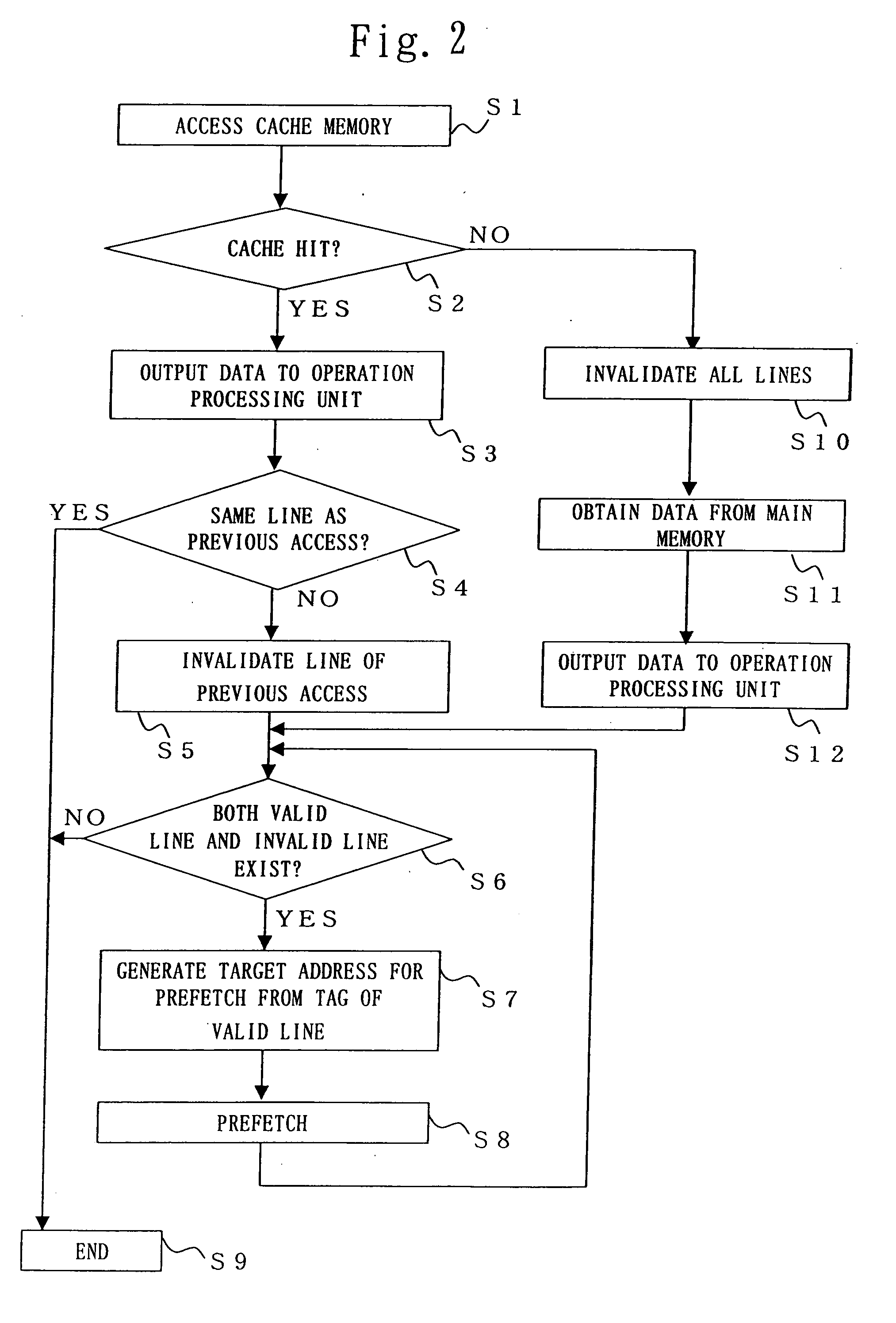
[0087] In the foregoing first embodiment, the prefetch is carried out when the operation processing unit 1 accesses the data of the cache line of the entry next to the cache line of the previous access.
[0088] In the third embodiment, another prefetching operation will be explained referring to FIG. 2 when the operation processing unit 1 accesses the data of the cache line of an entry located at some entries away from the cache line of the previous access instead of the cache line of the next entry, and a cache hit occurs.
[0089] Here, it is assumed that the cache memory 3 stores the data which has been stored subsequently to the data of the previous access in the main memory 7 in a valid status.
[0090] The operation processing unit 1 accesses the cache memory 3 (step S1), and the cache hit discriminating unit 2 discriminates if the cache memory 3 includes the target data accessed by the operation processing unit 1 (step S2).
[0091] When the cache memory 3 does not include the targe...
PUM
 Abstract
Description
Claims
Application Information
PatSnap Eureka turns technology decisions into work you can execute. Powered by our Innovation Knowledge Graph, it runs expert workflows across engineering, life sciences, materials and intellectual property. Get your review-ready output in minutes.


