Plasma etching method and plasma etching apparatus

A technology of plasma etching and processing method, which is applied in the direction of plasma, electrical components, discharge tubes, etc., and can solve problems such as poor

Active Publication Date: 2009-12-16
TOKYO ELECTRON LTD
View PDF6 Cites 0 Cited by
  • Summary
  • Abstract
  • Description
  • Claims
  • Application Information

AI Technical Summary

Problems solved by technology

It is necessary to adopt the above-mentioned ultra-low pressure process conditions, even if it is considered from the perspective of the best use of the equipment, it is not good

Method used


Image

  • Plasma etching method and plasma etching apparatus
  • Plasma etching method and plasma etching apparatus
  • Plasma etching method and plasma etching apparatus

Examples


Embodiment Construction

[0044] Hereinafter, embodiments of the present invention will be described with reference to the drawings.

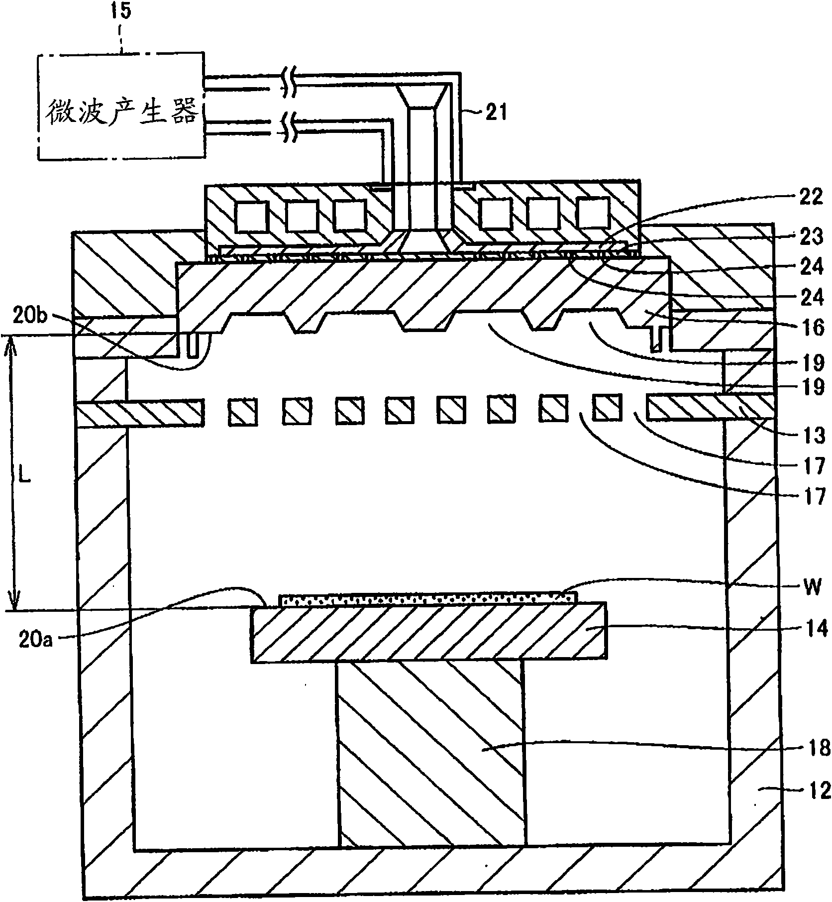
[0045] figure 1 It is a schematic sectional view showing main parts of a plasma etching processing apparatus according to an embodiment of the present invention. In addition, in the following drawings, the top in the sheet is regarded as the top.

[0046] refer to figure 1 , the plasma etching processing device 11 includes a processing container 12, a gas shower head 13, a holding table 14, a microwave generator 15, a dielectric plate 16, and a control unit (not shown); W performs plasma etching process; above-mentioned gas shower head 13 has a plurality of opening holes 17, as the reactive gas supply part that plasma etching process is supplied to processing container 12 with reactive gas; The bottom surface of the processing container 12 is provided on a support portion 18 extending upward, and the semiconductor substrate W is held on the holding table 14; the abov...


PUM


Abstract

Provided is a plasma etching method capable of controlling an etching shape readily and properly during a plasma etching process. The plasma etching method includes: holding a semiconductor substrate W on a holding table 14 installed in a processing chamber 12; generating a microwave for plasma ignition; generating plasma in the processing chamber 12 by setting a gap between the dielectric plate 16 and the holding table 14 to be equal to or greater than about 100 mm and setting a pressure inside the processing chamber 12 to be equal to or higher than about 50 mTorr, and introducing the microwave into the processing chamber 12 via the dielectric plate 16; and performing a plasma etching process on the semiconductor substrate W by the plasma generated by supplying a reactant gas for plasma etching process into the processing chamber 12.

Description

technical field [0001] The present invention relates to a plasma etching treatment method and a plasma etching treatment apparatus, and particularly to a plasma etching treatment method and a plasma etching treatment apparatus used in a semiconductor device manufacturing process. Background technique [0002] Semiconductor devices such as LSI (Large Scale Integrated Circuit) are manufactured by performing various processes such as etching, CVD (Chemical Vapor Deposition), and sputtering on a semiconductor substrate. Regarding processes such as etching, CVD, and sputtering, there are processing methods using plasma as an energy supply source, that is, plasma etching, plasma CVD, and plasma sputtering. [0003] With recent miniaturization and multilayer wiring of LSIs, the above-mentioned plasma treatment is effectively utilized in each process of manufacturing a semiconductor device. For example, in plasma processing in the manufacturing process of semiconductor devices such...

Claims


Application Information

Patent Timeline
Patent Type & Authority Applications(China)
IPC IPC(8): H01L21/3065H01L21/311H01L21/3213C23F4/00H05H1/24H01L21/00
CPCH01J37/3244H01L21/3065H01J37/32449H01J37/32192
Inventor 佐佐木胜
Owner TOKYO ELECTRON LTD
Why Eureka
Try Eureka