The method of removing dummy gate

A dummy gate and wet etching technology, applied in semiconductor devices, electrical components, circuits, etc., can solve problems affecting transistor performance, substrate damage, etc., achieve low electron temperature, not easy to damage, and reduce accumulation effects

Active Publication Date: 2019-01-22
SEMICON MFG SOUTH CHINA CORP
View PDF7 Cites 0 Cited by
  • Summary
  • Abstract
  • Description
  • Claims
  • Application Information

AI Technical Summary

Problems solved by technology

[0003] In the prior art, plasma etching and wet etching are generally used to remove dummy gates in sequence, wherein plasma etching removes more than half of the dummy gates, and the process of removing dummy gates by plasma etching may cause damage to the substrate. thereby affecting the performance of transistors formed on the substrate

Method used


Image

  • The method of removing dummy gate
  • The method of removing dummy gate
  • The method of removing dummy gate

Examples


Embodiment Construction

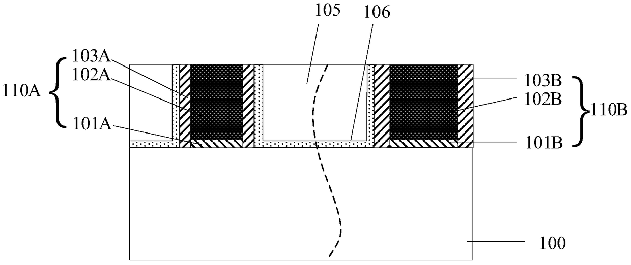
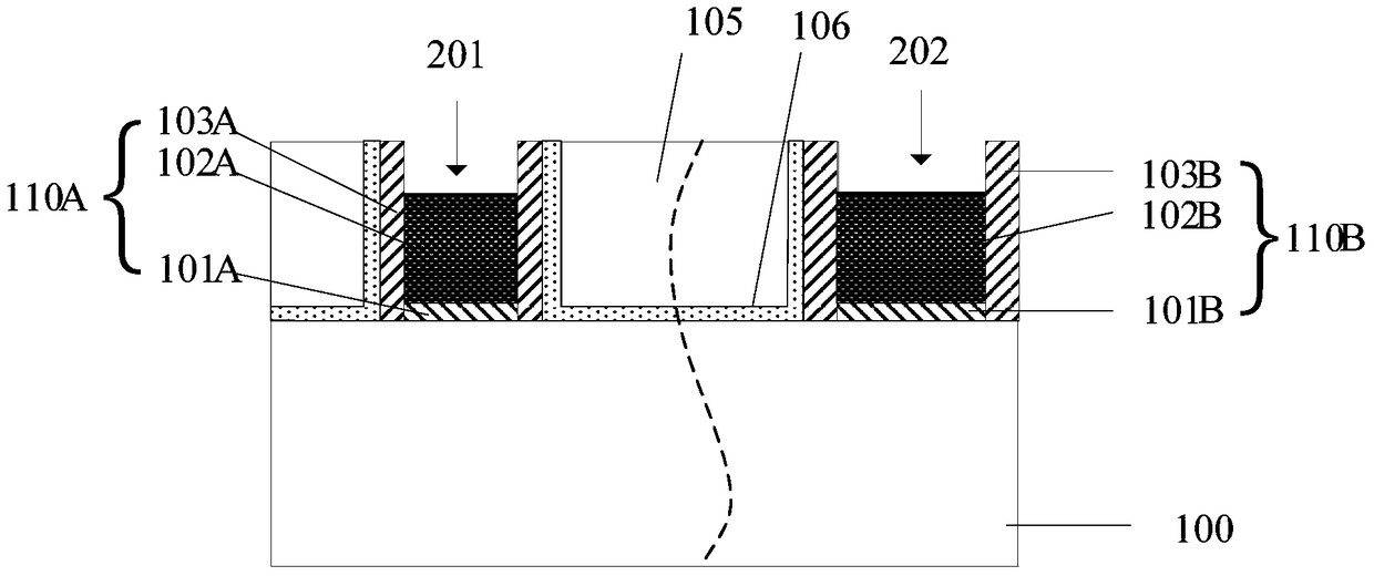
[0027] In the prior art, plasma etching and wet etching are generally performed in sequence to remove the dummy gates, wherein the plasma etching causes relatively large damage to the substrate.

[0028] The damage to the substrate can be roughly divided into two types: the damage to the substrate performance and the damage to the substrate morphology, and the damage to the substrate morphology will also affect the performance of the substrate. In the process of plasma etching, the plasma with high electron temperature easily enters the substrate under the dummy gate, which affects the performance of the carrier distribution in the substrate such as holes, thereby affecting the performance of the transistor; The vacuum ultraviolet (Vacuum Ultraviolet, VUV) generated by the plasma etching process irradiates the semiconductor substrate, which will also cause damage to the substrate performance; in addition, plasma etching has different etching rates for dummy gates of different s...


PUM


Abstract

The invention provides a method for removing pseudo grids, and the method comprises the steps: carrying out the first etching of the pseudo grids through employing pulse plasma etching at a step of pseudo grid removal, and removing the pseudo grids at a certain height; carrying out the second etching of the pseudo grids through employing surface wave plasma etching, and removing the pseudo grids at a certain height; carrying out the third etching of the pseudo grids through employing wet etching, removing the pseudo grids, and enabling an opening to be exposed out of a substrate. The method employs the pulse plasma etching to carry out the first etching of the pseudo grids, and the thickness of larger pseudo grids is basically the same as the thickness of smaller pseudo grids after the first etching, thereby enabling plasma finally generated through surface wave plasma etching to be lower in electron temperature and to be not liable to enter into the substrate in a process of the second etching of the remaining pseudo grids through employing the surface wave plasma. Meanwhile, vacuum ultraviolet light generated by surface wave plasma etching is little, thereby causing little damage to the substrate.

Description

technical field [0001] The present invention relates to the field of semiconductors, in particular to a method for removing dummy gates. Background technique [0002] In the high-K dielectric / metal-last process of transistors, after high-temperature annealing for ion activation, it is necessary to remove dummy gates (such as polysilicon gates) to form openings, and then fill the openings with metal to form metal gates to form high-K Dielectric / Gate-last structure. [0003] In the prior art, plasma etching and wet etching are generally used to remove dummy gates in sequence, wherein plasma etching removes more than half of the dummy gates, and the process of removing dummy gates by plasma etching may cause damage to the substrate. This affects the performance of transistors formed on the substrate. [0004] Therefore, there is an urgent need for a method for removing the dummy gate, which reduces damage to the substrate under the dummy gate when removing the dummy gate, the...

Claims


Application Information

Patent Timeline
Patent Type & Authority Patents(China)
IPC IPC(8): H01L21/311H01L21/28
Inventor 张海洋张城龙
Owner SEMICON MFG SOUTH CHINA CORP
Why Eureka
Try Eureka