Silicon oxide film forming method and semiconductor device manufacturing method

一种氧化膜、半导体的技术,应用在半导体/固态器件制造、半导体器件、晶体管等方向,能够解决氧化速率的条件研究等问题

Inactive Publication Date: 2010-02-03
TOKYO ELECTRON LTD
View PDF5 Cites 0 Cited by
  • Summary
  • Abstract
  • Description
  • Claims
  • Application Information

AI Technical Summary

Problems solved by technology

However, in the methods of the above-mentioned Patent Documents 1 and 2, the film quality of the oxide film is mainly improved, so the conditions for increasing the oxidation rate have not been studied.

Method used


Image

  • Silicon oxide film forming method and semiconductor device manufacturing method
  • Silicon oxide film forming method and semiconductor device manufacturing method
  • Silicon oxide film forming method and semiconductor device manufacturing method

Examples


Embodiment Construction

[0067] Hereinafter, the best mode of the present invention will be described with reference to the drawings.

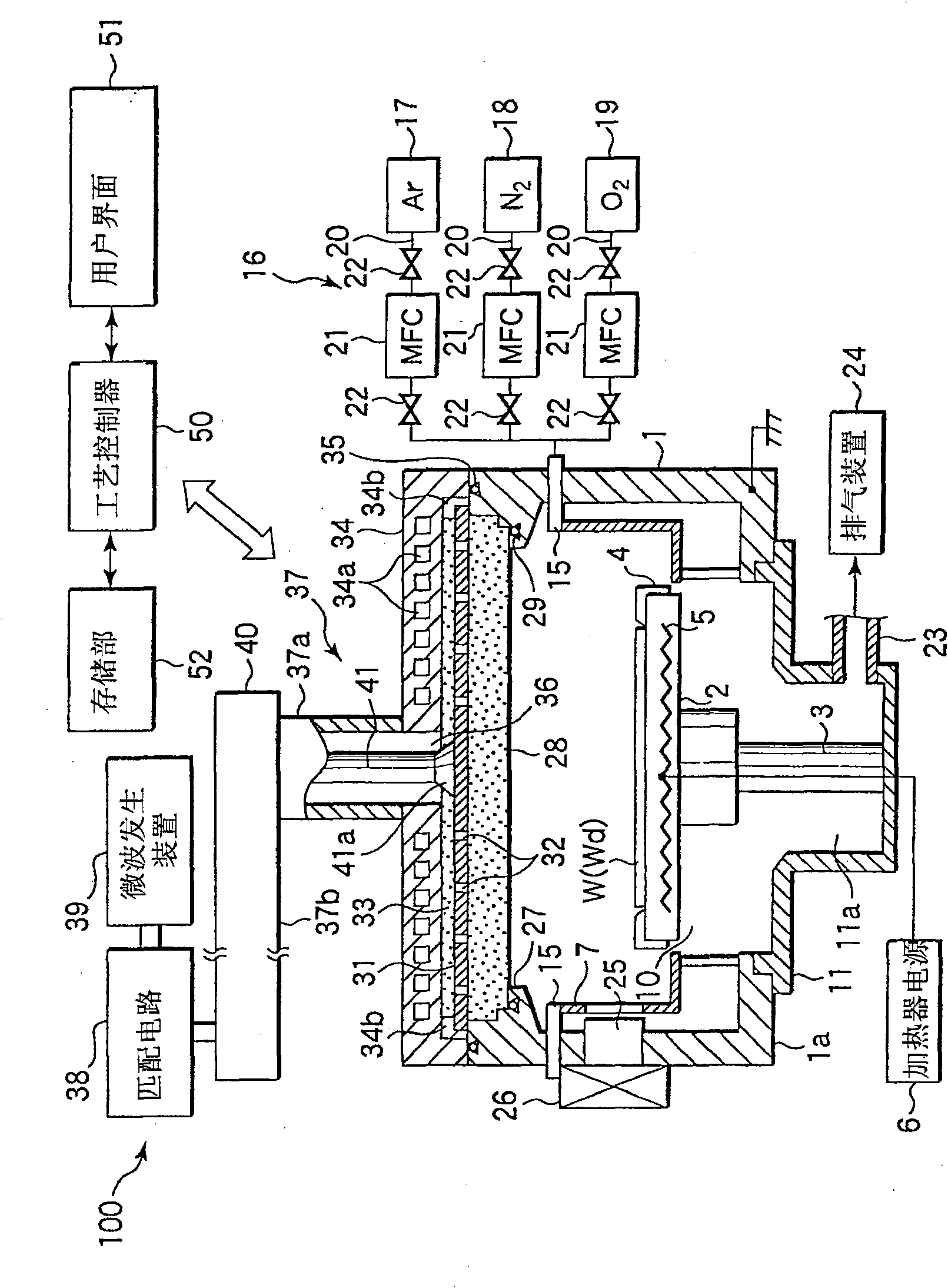
[0068] figure 1 It is a schematic cross-sectional view of an example of a plasma processing apparatus suitable for carrying out the method for forming an oxide film according to the present invention. This plasma processing apparatus utilizes the RLSA (Radial Line Slot Antenna; Radial Line Slot Antenna) plasma generation technology in which microwaves are introduced into the processing chamber through a planar antenna with a plurality of slots to generate plasma. microwave plasma.

[0069] The plasma processing device 100 can use plasma with a low electron temperature to perform plasma processing without damage to the bottom film at a low temperature below 600 degrees. At the same time, it can also achieve good plasma uniformity. Compared with the dense oxide film and the uniformity of the process, it is not inferior. Therefore, the plasma oxidation treatment appa...


PUM


Abstract

A plasma processing apparatus 100 of the RLSA type includes a planar antenna with a plurality of slots formed therein, by which microwaves are supplied into a process chamber to generate plasma. In this apparatus, poly-silicon oxidation is performed at a pressure of 67 to 667 Pa inside the chamber, a temperature of 300 to 600 C, and a microwave power of 1,000 to 3,500W, while a process gas containing Ar gas at a rate of 100 to 2,000 mL / min and O 2 gas at a rate of 1 to 500 mL / min is used with O 2 gas / Ar gas ratio set to be 0.5 to 5%.

Description

technical field [0001] The present invention relates to a method of forming an oxide film and a method of manufacturing a semiconductor device when manufacturing a semiconductor device such as a flash memory element or a thin film transistor. Background technique [0002] Various semiconductor devices, such as silicon semiconductor flash memory elements or thin-film transistors used in LCDs (liquid crystal displays), generally use methods such as thermal oxidation or CVD to form oxide films for the purpose of insulating gate electrodes. And formed. In the past, since the thermal oxidation film obtained by thermal oxidation of silicon or polycrystalline silicon (polycrystalline silicon) was superior in film quality compared with other methods, dry-O 2 Or a wet (Wet) thermal oxidation method such as WVG (Water Vapor Generation) or ISSG (In Situ Steam Generation). [0003] However, since the thermal oxidation method heats polysilicon to a high temperature of 900-1000° C. in a...

Claims


Application Information

Patent Timeline
Patent Type & Authority Patents(China)
IPC IPC(8): H01L21/316H01L21/318H01L21/336H01L21/8247H01L27/115H01L29/786H01L29/788H01L29/792
CPCH01L21/02274H01L21/32105H01L21/31612H01L21/28282H01L21/0217H01L21/28273H01L21/022H01L21/02164H01J37/32935H01J37/32192H01L29/40114H01L29/40117
Inventor 小林岳志北川淳一
Owner TOKYO ELECTRON LTD
Why Eureka
Try Eureka