Method of forming mos transistor and method of forming cmos transistor

A MOS transistor and transistor technology, applied in the formation of MOS transistors and CMOS transistors, can solve the problems of performance degradation of semiconductor devices and differences in threshold voltages of different MOS transistors, and prevent the generation of pollutants, low electron temperature, and damage small effect

Active Publication Date: 2018-11-16
SEMICON MFG INT (SHANGHAI) CORP
View PDF4 Cites 0 Cited by
  • Summary
  • Abstract
  • Description
  • Claims
  • Application Information

AI Technical Summary

Problems solved by technology

[0007] Due to the existing method of forming MOS transistors, openings with different depths will be formed after removing the dummy gates with different widths, resulting in differences in the threshold voltages of different MOS transistors that are finally formed, degrading the performance of semiconductor devices
The same problem exists in the formation of CMOS transistors

Method used


Image

  • Method of forming mos transistor and method of forming cmos transistor
  • Method of forming mos transistor and method of forming cmos transistor
  • Method of forming mos transistor and method of forming cmos transistor

Examples


Embodiment Construction

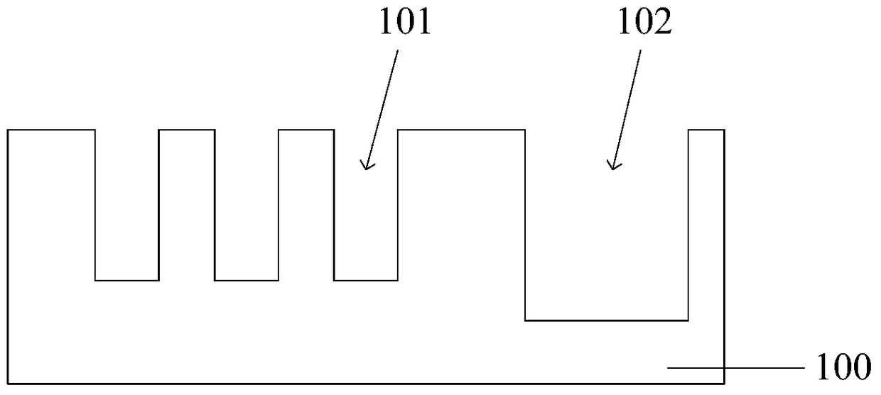
[0052] As described in the background art, the existing method uses a continuous wave plasma etching process to remove the dummy gate. Since the continuous wave plasma has different etching rates for dummy gates of different widths, the formed opening depths are different. Various problems, such as unclean removal of the dummy gate in some locations, and damage to the structure under the dummy gate in some locations, occur.

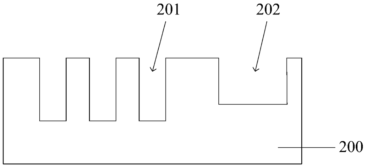
[0053] For this reason, the present invention proposes to adopt a pulse plasma etching process to remove the dummy gate to form an opening. Since the pulse plasma is etched at a certain frequency, there is a short pause time after each etching. During the pause time, the etching product It can be evenly dispersed and provide the same environment for the next frequency of etching, thereby ensuring that the formed openings have the same depth.

[0054] In order to make the above-mentioned objects, features and advantages of the present invention more obvious and...


PUM


Abstract

The present invention relates to a formation method of an MOS transistor and a formation method of a CMOS transistor, wherein the formation method of the MOS transistor comprises the steps of providing a semiconductor substrate, wherein the semiconductor substrate is equipped with a pseudo gate; forming a source region and a drain region in the semiconductor substrate below the two sides of the pseudo gate respectively; forming an interlayer dielectric layer on the semiconductor substrate, wherein the upper surface of the interlayer dielectric layer is parallel and level with the upper surface of the pseudo gate; adopting a pulse plasma etching technology to remove the pseudo gate to form an opening; adopting a metal material to fill the opening to form a metal gate. The performance of the MOS transistor formed by the formation method of the MOS transistor is improved.

Description

Technical field [0001] The present invention relates to the field of semiconductor manufacturing, in particular to a method for forming a MOS transistor and a method for forming a CMOS transistor. Background technique [0002] With the continuous development of semiconductor manufacturing processes, the critical dimensions (Critical Dimension, CD) of semiconductor devices in integrated circuits are getting smaller and smaller. In order to solve a series of problems caused by small-sized devices, the use of high dielectric constant (k) materials The technology of combining a gate dielectric layer and a metal gate is introduced into the manufacturing process of MOS transistors. [0003] In order to avoid the influence of the metal material of the metal gate on other structures of the MOS transistor, the gate stack structure of the metal gate and the high-k gate dielectric layer is usually made by a gate-last process. In this process, a dummy gate made of polysilicon and other materi...

Claims


Application Information

Patent Timeline
Patent Type & Authority Patents(China)
IPC IPC(8): H01L21/336H01L21/28H01L21/8238
Inventor 张海洋尚飞
Owner SEMICON MFG INT (SHANGHAI) CORP
Why Eureka
Try Eureka