A plasma processing device

A plasma and processing device technology, applied in the field of plasma processing devices, can solve problems such as substrate damage, inability to adapt to semiconductor manufacturing processes, and limited application range, and achieve high density, precise processing, and low electron temperature.

Active Publication Date: 2019-01-22
SEMICON MFG INT (SHANGHAI) CORP +1
View PDF4 Cites 0 Cited by
  • Summary
  • Abstract
  • Description
  • Claims
  • Application Information

AI Technical Summary

Problems solved by technology

[0002] Plasma processing is an indispensable technology in the manufacture of semiconductors. Currently, capacitively coupled and inductively coupled plasma processing devices are commonly used. Due to the high temperature of the electrons, it is easy to cause damage to the substrate.
With the shrinking of the size of semiconductor devices, the current ion plasma processing device has gradually been unable to adapt to the semiconductor manufacturing process of smaller technology nodes. For technology nodes of 14nm and below, RLSA (Radial Line Slot Antenna) driven Surface wave plasma (SWP, surface wave plasma) has attracted extensive attention because of its small damage to the substrate.
[0003] However, due to the RLSA surface wave plasma processing device, since the energy range of the surface wave plasma mainly depends on the microwave, its application range is limited.

Method used


Image

  • A plasma processing device
  • A plasma processing device
  • A plasma processing device

Examples


Embodiment 1

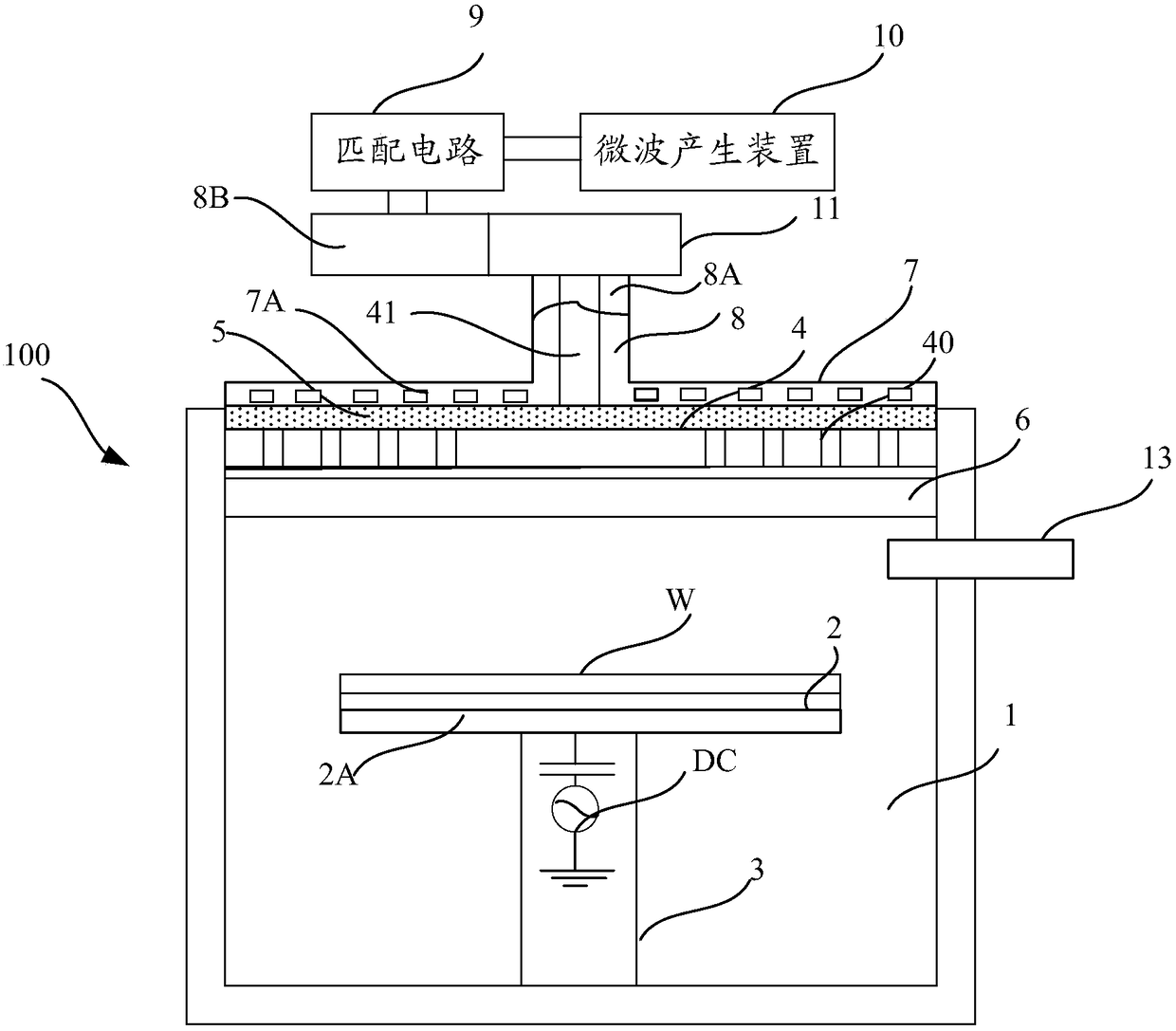
[0025] figure 1 A schematic structural diagram of a plasma processing apparatus according to an embodiment of the present invention is shown. The plasma processing device is a RLSA surface wave plasma processing device, which uses a planar antenna with a plurality of slits, especially a RLSA (Radial Line Slot Antenna) to introduce microwaves into the processing chamber, by This can generate surface wave plasma with high density and low electron temperature, and various plasma treatments, such as plasma oxidation treatment and etching, can be implemented by means of the surface wave plasma.

[0026] Such as figure 1 As shown, the plasma processing apparatus 100 has a processing chamber 1 that is a substantially cylindrical chamber 1 that is hermetically sealed and grounded. An electrostatic chuck 2 made of ceramics such as AlN for horizontally supporting an object to be processed such as a semiconductor wafer (hereinafter simply referred to as "wafer") W is provided in the pr...

Embodiment 2

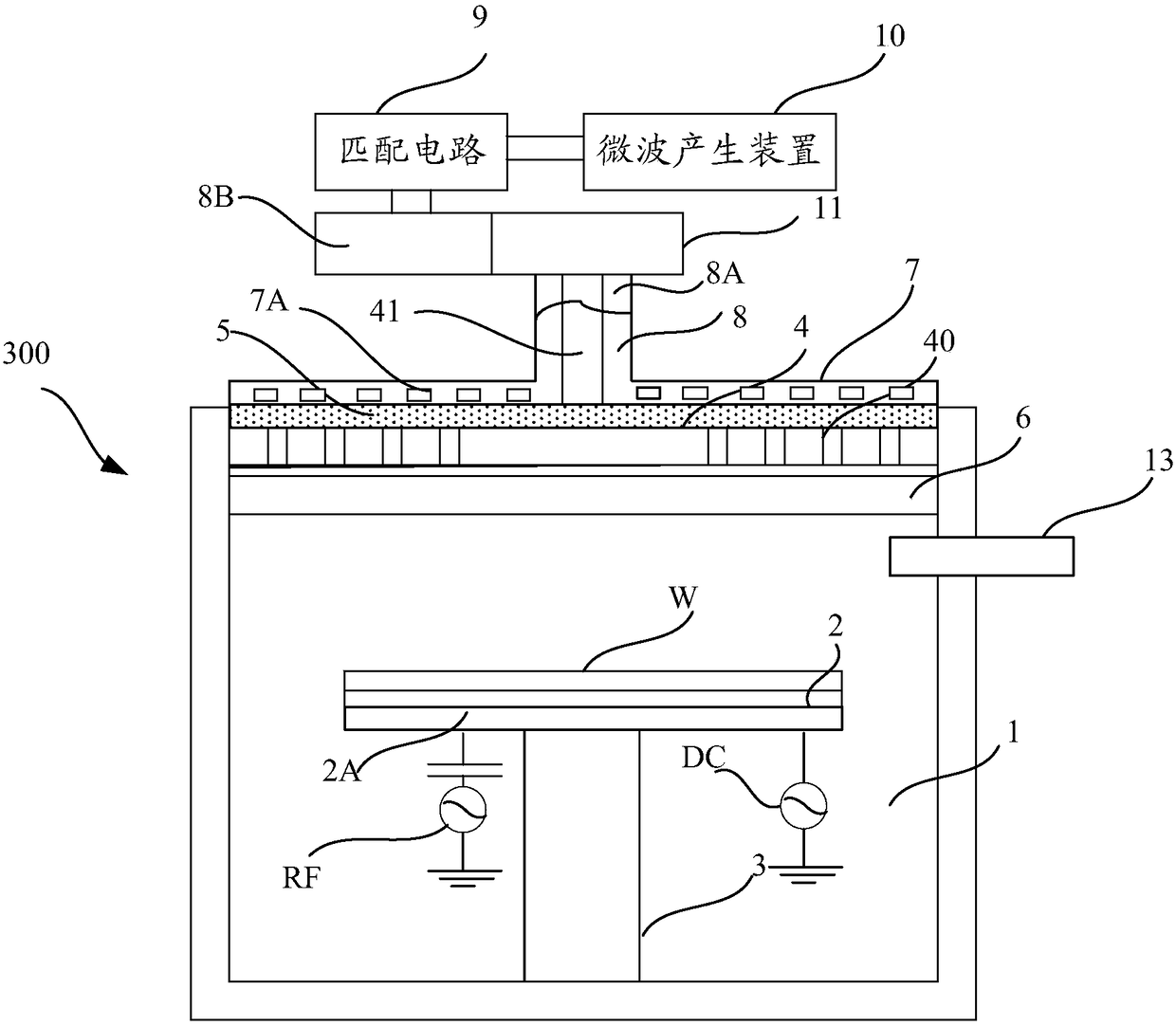
[0040] image 3 A schematic structural diagram of a plasma processing apparatus according to another embodiment of the present invention is shown. The plasma processing device is also an RLSA surface wave plasma processing device, and the RLSA surface wave plasma processing device 300 and figure 1 The shown surface wave plasma processing device 100 is similar, except that, in this embodiment, on the lower electrode plate 2A, in addition to the DC bias, a radio frequency bias RF is also applied, and the radio frequency bias RF The pulse of the microwave is synchronized with the microwave pulse generated by the microwave generating device 10, that is, the phases of the two are the same, as Figure 4 Shown in curve 1 and curve 2.

[0041] Exemplarily, in this embodiment, the frequency of the radio frequency bias RF is 13.56 MHz, which is generated by a radio frequency pulse sending device commonly used in the field, and will not be repeated here. It can be understood that, in ...


PUM


Abstract

The invention provides a plasma processing device, which relates to the technical field of semiconductors. The plasma processing device comprises a processing cavity, an electrostatic chuck, a microwave generating device, a planar antenna, a dielectric plate and a lower electrode plate, wherein the electrostatic chuck is arranged in the processing cavity for bearing a to-be-processed plasma; the microwave generating device is used for generating microwaves and guiding the microwaves to the processing cavity through a guiding tube; the planar antenna is composed of a conductor and is provided with multiple slits for radiating the microwaves guided by the guiding tube to the processing cavity; the dielectric plate is composed of a dielectric and forms the top wall of the processing cavity for enabling the microwaves passing through the slits of the planar antenna to pass through; and DC bias voltage is applied to the lower electrode plate for adjusting the energy of surface wave plasmas. The plasma processing device of the invention has the advantages that the plasma density is high; the electron temperature is low; precise processing can be realized; or high selectivity in plasma etching can be realized.

Description

technical field [0001] The present invention relates to the technical field of semiconductors, in particular to a plasma processing device. Background technique [0002] Plasma processing is an indispensable technology in the manufacture of semiconductors. Currently, capacitively coupled and inductively coupled plasma processing devices are commonly used, and the substrate is easily damaged due to the high temperature of the electrons. With the shrinking of the size of semiconductor devices, the current ion plasma processing device has gradually been unable to adapt to the semiconductor manufacturing process of smaller technology nodes. For technology nodes of 14nm and below, RLSA (Radial Line Slot Antenna) driven Surface wave plasma (SWP, surface wave plasma) has attracted extensive attention because of its less damage to the substrate. [0003] However, due to the RLSA surface wave plasma processing device, the energy range of the surface wave plasma mainly depends on the...

Claims


Application Information

Patent Timeline
Patent Type & Authority Patents(China)
IPC IPC(8): H01J37/32
CPCH01J37/32284
Inventor 张海洋张城龙袁光杰
Owner SEMICON MFG INT (SHANGHAI) CORP
Why Eureka
Try Eureka