Electrical wiring design for module removal and replacement from organic board

a technology of electrical wiring and organic boards, applied in the field of reworkable and removable encapsulated integrated circuit chips, can solve the problems of local hot spots across the board, components may need to be separated from one another, and certain components within the assembly may be undetected from one another,

Inactive Publication Date: 2006-09-14
GOOGLE LLC
View PDF18 Cites 34 Cited by
  • Summary
  • Abstract
  • Description
  • Claims
  • Application Information

AI Technical Summary

Benefits of technology

[0018] The above and other objects, which will be apparent to those skilled in art, are achieved in the present invention, which is directed to a method for separating electronic components joined by solder interconnections. The method includes providing a chip carrier joined to a substrate via a solder interconnection, whereby the chip carrier has an electrical heating component with a planar surface adjacent to the solder interconnection. Resistive heat is generated within the electrical heating component, and this resistive heat is transferred to the solder interconnection to allow for localized melting of the solder interconnection and removal of the chip carrier from the substrate without affecting other components residing on the substrate.

Problems solved by technology

However, once the solder interconnections are completed, the components may need to be detached from one another.
However, by externally applying heat to the electrical component, and optionally the underside of the organic board, certain components within the assembly may be undesirably heated beyond their sustainable temperatures.
This external heat may also lead to local hot spots across the board since the hot gas is directed locally on the module that needs to be removed there from.
Locally applied heat can also lead to warpage of the organic board as a result of the non-uniform heating of such board.
This is undesirable as any board warpage may require that the board be scrapped, along with several other good modules / passives / devices on the board.
Further adding to the problems associated with warpage is the placement of heater blocks, or heating units, at the backside of the board as they often interfere with the requirement of holding the board firm and flat.
The above problems only get worse as the board size and thickness increase, or when removing large electrical components for rework, such as those having high thermal masses.
Yet, these higher rework temperatures for lead free solders can irreparably damage the organic board, and as such, rework of lead free alloy containing assemblies has become a critical issue in the qualification of this technology.

Method used


Image

  • Electrical wiring design for module removal and replacement from organic board
  • Electrical wiring design for module removal and replacement from organic board
  • Electrical wiring design for module removal and replacement from organic board

Examples


Embodiment Construction

)

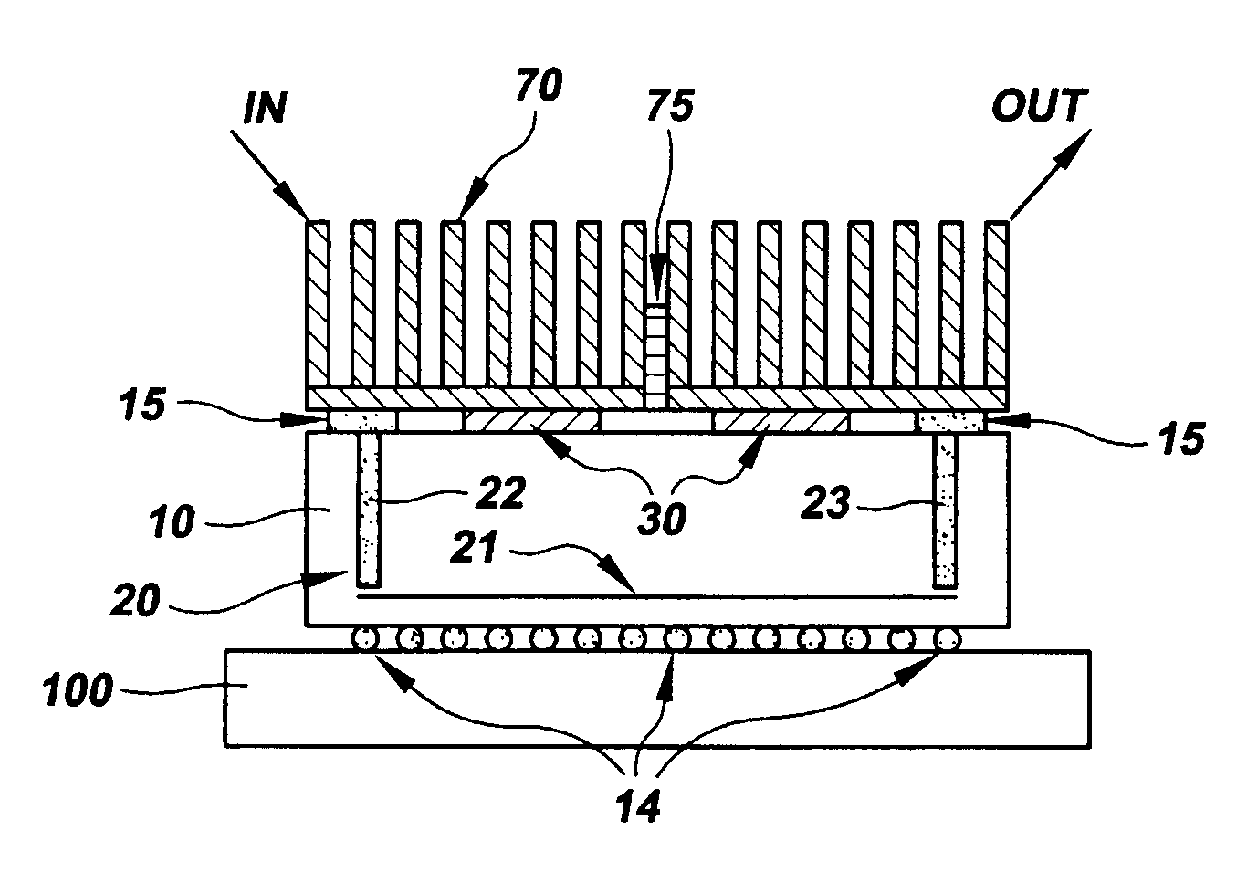
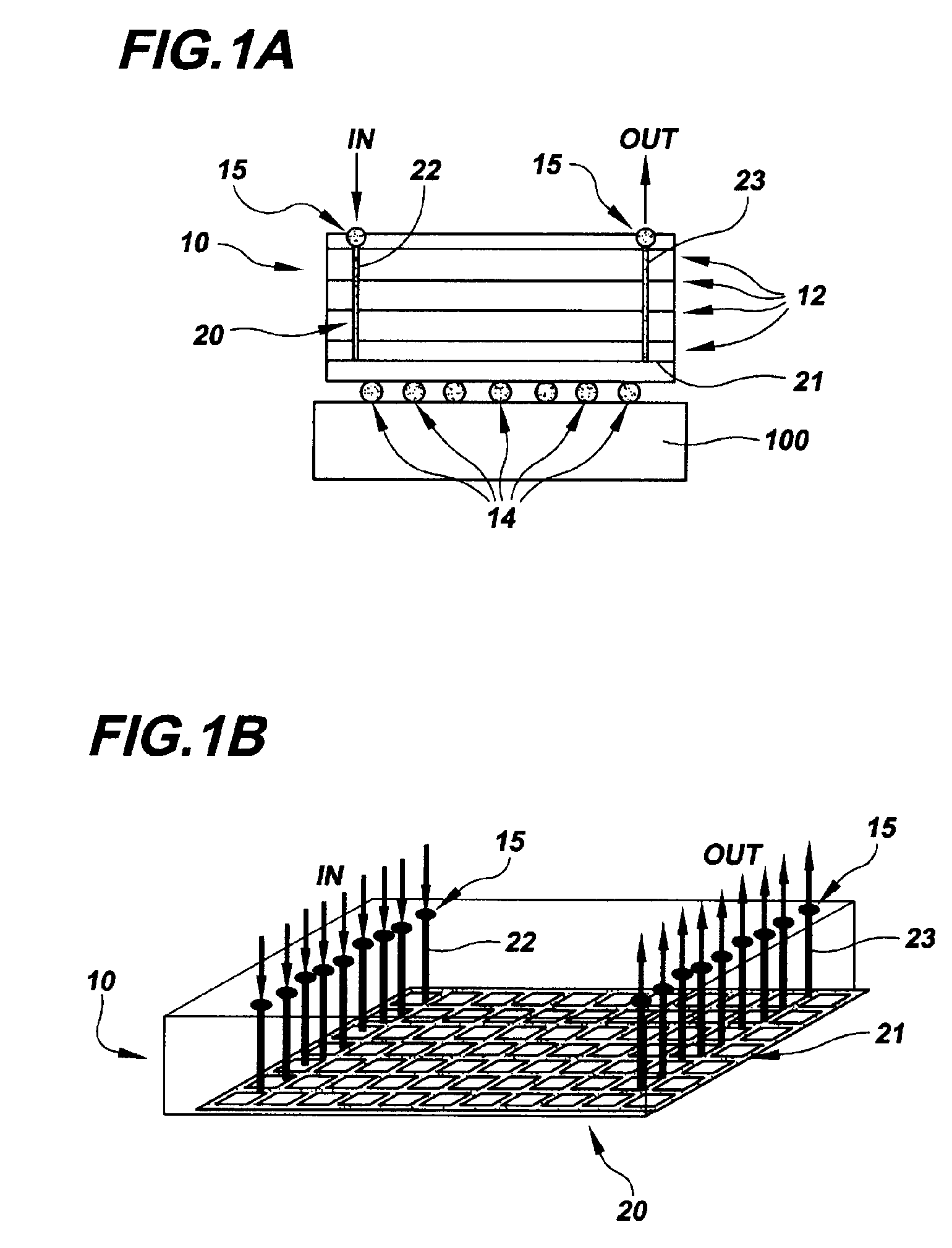
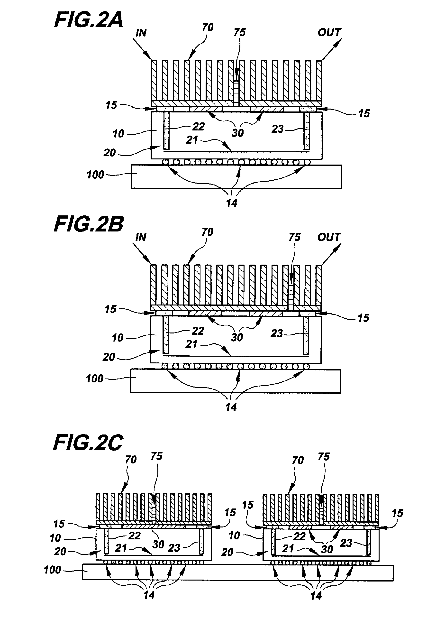
[0033] In describing the preferred embodiment of the present invention, reference will be made herein to FIGS. 1A-3C of the drawings in which like numerals refer to like features of the invention.

[0034] The present invention provides for the removal and rework of electrical modules joined to a board or substrate via solder interconnections. The invention advantageously uses the electrical design of the electrical module itself to create wiring channels within the package. The wiring channels may use an existing electrical component within the module, or they may modify or add to the existing electrical design of the module. Preferably, the wiring channels use existing mesh planes or slightly modified mesh planes residing within the module. The wiring channels transfer the required levels of electric current to the joint interface adjacent the solder interconnections. This current is used to create Joule heating (I2R) at the joint interface to melt the solder interconnections and a...


PUM

PropertyMeasurementUnit
alternating frequenciesaaaaaaaaaa
temperaturesaaaaaaaaaa

Abstract

A method and electrical structure for separating electronic components from one another joined by solder interconnections. An electronic module is joined to a substrate via a solder interconnection, whereby the electronic module has an electrical heating component residing within a bottom layer thereof adjacent a solder interconnection. Preferably, a chip carrier is joined to a board whereby the chip carrier has an electrical mesh plane for heating adjacent the solder interconnection. Resistive heat is generated within this electrical heating component either by applying an electrical current to the electrical heating component, or by non-contact inductively heating the layer in which such electrical heating component resides to generate resistive heat within the electrical heating component. The resistive heat is transferred to the solder interconnection to allow for localized melting of the solder interconnection and removal of the electronic components from one another.

Description

BACKGROUND OF THE INVENTION [0001] 1. Field of the Invention [0002] The present invention relates to electronic devices, and in particular, to removable and reworkable encapsulated integrated circuit chips and the method of manufacture. [0003] 2. Description of Related Art [0004] Surface mount technology (SMT) is a known fabrication process in the microelectronics industry. SMT generally involves forming electronic package assemblies whereby an electrical component, such as an integrated circuit chip, is electrically and mechanically connected to a substrate, a card (i.e., board), another chip or another electronic part. [0005] In one particular application, to which this application is directed to for convenience, multilayer glass-ceramic components, as exemplified by integrated circuit chips on ceramic chip carriers, are joined to printed circuit boards (cards) and / or organic substrates. Often, these multilayer glass-ceramic electronic components are joined to other components by ...

Claims


Application Information

Patent Timeline
Patent Type & Authority Applications(United States)
IPC IPC(8): B23K31/02
CPCB23K1/018Y10T29/49819H01L24/98H01L2224/81222H01L2224/81234H01L2924/01029H01L2924/01082H01L2924/09701H05K1/0212H05K3/3436H05K3/3494H05K2203/176H01L2924/01006H01L2924/01033H01L2924/01042H01L2924/01047H01L2924/01074H01L2924/01075H01L2924/01322H01L2924/10253B23K2201/40Y10T29/49721Y10T29/49144Y10T29/49815Y10T29/49821H01L2924/00B23K2101/40H01L2924/14
Inventor FAROOQ, MUKTA G.HAMEL, HARVEY C.
Owner GOOGLE LLC
Why Eureka
Try Eureka