Supercharge Your Innovation With Domain-Expert AI Agents!

Array substrate for lcd

Active Publication Date: 2006-09-14
SAMSUNG DISPLAY CO LTD
View PDF6 Cites 9 Cited by
  • Summary
  • Abstract
  • Description
  • Claims
  • Application Information

AI Technical Summary

Benefits of technology

[0019] According to the present invention, the bonding of a color filter substrate and an array substrate is reinforced.
[0020] Furthermore, a liquid crystal material is completely filled in between the color filter substrate and the array substrate, which increases the productivity.

Problems solved by technology

Furthermore, the light leakage between the data line and the pixel electrode causes lower luminance.
Furthermore, when the insulation layer is formed, the distance between the data line and the pixel electrode increases.
Therefore, even when a portion of the data line overlaps with the pixel electrode, a parasitic capacitance formed between the data line and the pixel electrode becomes negligibly small.
However, when the insulation layer is formed, the bonding strength between the sealant that combines the color filter substrate and the array substrate, and the insulation layer, or the bonding strength between the insulation layer and the gate insulation layer becomes fragile.
Even though the color filter substrate is not completely separated from the array substrate, liquid crystal material is not completely injected into between the color filter substrate and the array substrate due to the crack formed between the sealant and the insulation layer or between the insulation layer and the gate insulation layer, which lowers the productivity.

Method used


Image

  • Array substrate for lcd
  • Array substrate for lcd
  • Array substrate for lcd

Examples


Embodiment Construction

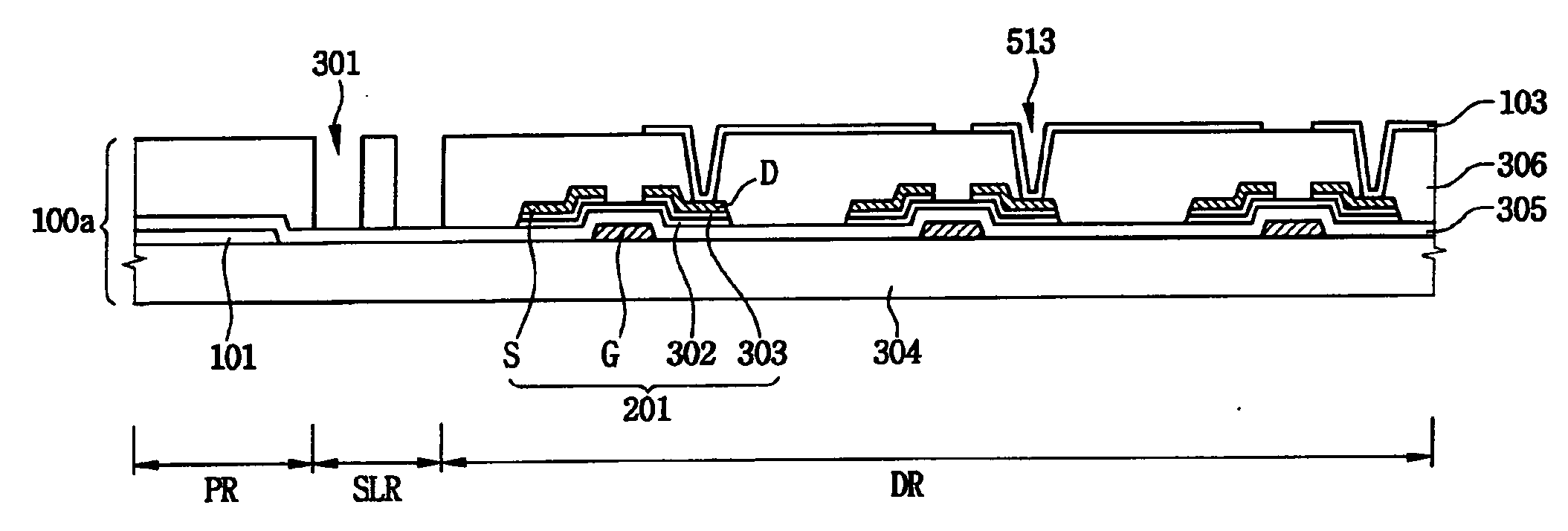
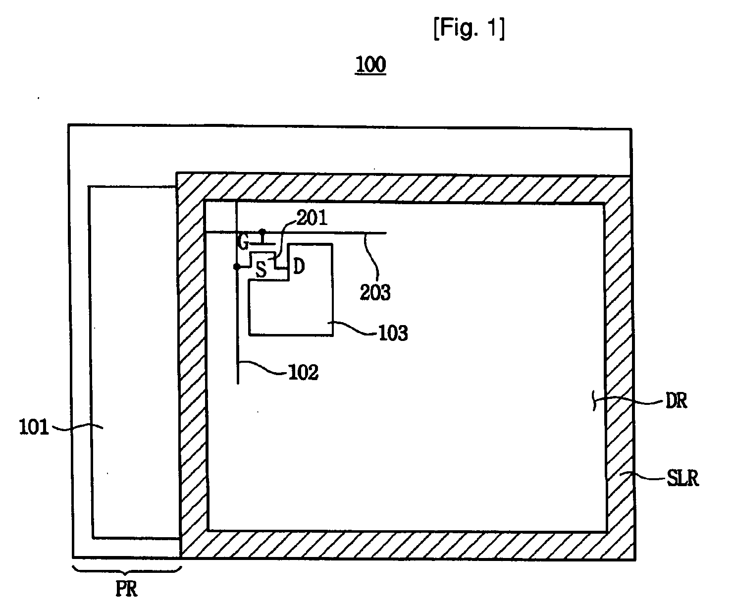
[0029]FIG. 1 is a schematic plan view showing an array substrate.

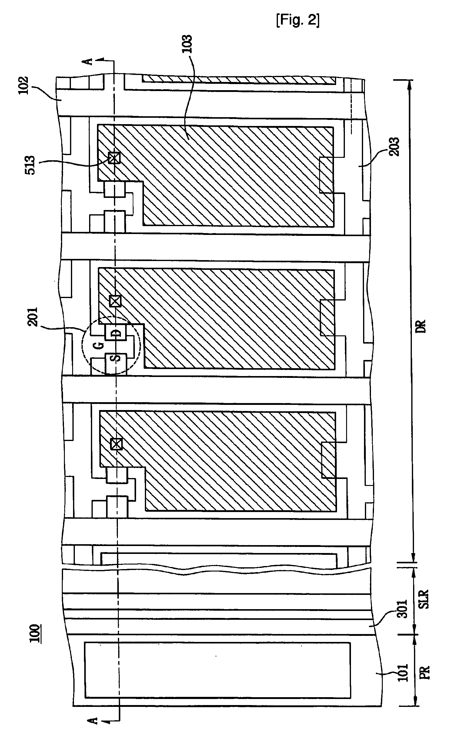
[0030] Referring to FIG. 1, an array substrate 100 includes a display region DR and a peripheral region PR. The display region DR displays an image, and the peripheral region includes a driving circuit, such as a gate driving circuit 101. A data driving circuit (not shown) is made in the form of separate chip, and the data driving circuit is electrically connected to the array substrate 100. The data driving circuit is also disposed on the peripheral region PR.

[0031] A sealine region SLR is disposed between the display region DR and the peripheral region PR, such that the sealine region SLR divides the display region DR and the peripheral region PR. A sealing member (not shown) for bonding the array substrate and a color filter substrate (not shown) is to be disposed on the sealine region SLR.

[0032] The display region DR includes a plurality of gate lines 203 arranged in parallel each other, and a plurality of data ...


PUM


Abstract

An array substrate (100a) includes a transparent substrate (304), a first insulation layer (306) and a pixel electrode (103). The transparent substrate (304) includes a display region (DR) that displays an image, a peripheral region (PR) having a driving circuit (101) for displaying an image through the display region, and a sealine region (SLR) that surrounds the display region (DR) to define the display region and the peripheral region (PR). The first insulation layer (306) is formed over the transparent substrate (304), and the first insulation layer (306) has an opening window (301) in the sealine region (SLR). The pixel electrode (103) is formed on the first insulation layer (306) of the display region (DR). The bonding between a color filter substrate (401) and an array substrate (100a) is improved. Furthermore, liquid crystal material is completely filled into between the color filter substrate and the array substrate.

Description

TECHNICAL FIELD [0001] The present invention relates to an array substrate, a method of manufacturing the array substrate, a liquid crystal display apparatus having the arrays substrate and a method of manufacturing the liquid crystal display apparatus. More particularly, the present invention relates to an array substrate for a strong bonding with a color filter substrate, a method of manufacturing the array substrate, a liquid crystal display apparatus having the arrays substrate and a method of manufacturing the liquid crystal display apparatus. BACKGROUND ART [0002] Recently, a liquid crystal display apparatus is widely used, because the liquid crystal display apparatus has lightweight, thin thickness and low power consumption. [0003] The liquid crystal display apparatus includes a liquid crystal display panel and a backlight assembly. The backlight assembly provides light to the liquid crystal display panel. The liquid crystal display panel includes a color filter substrate and...

Claims


Application Information

Patent Timeline
IPC IPC(8): G02F1/1339G02F1/1333G02F1/1341
CPCG02F1/1339G02F1/1341G02F1/1333
Inventor SONG, YOUNG-GOOKONG, HYANG-SHIKKIM, SUNG-MAN
Owner SAMSUNG DISPLAY CO LTD
Features
  • R&D
  • Intellectual Property
  • Life Sciences
  • Materials
  • Tech Scout
  • Unparalleled Data Quality
  • Higher Quality Content
  • 60% Fewer Hallucinations
Learn More