Semiconductor designing apparatus

a design apparatus and semiconductor technology, applied in the field of semiconductor device design, can solve the problems of inability to confirm a circuit having the difference on the circuit diagram, and long time taken for detecting a difference, so as to prevent the execution of simulation, shorten the time taken for analyzing, and prevent the effect of simulation execution error

Inactive Publication Date: 2006-09-14
PANASONIC CORP
View PDF16 Cites 35 Cited by
  • Summary
  • Abstract
  • Description
  • Claims
  • Application Information

AI Technical Summary

Benefits of technology

[0042] According to the invention, furthermore, it is possible to confirm, over a circuit diagram, the simulation mode to be used in each block before the execution of the simulation. Consequently, there is an advantage that it is possible to prevent the execution of the simulation in an execution mode which is not intended before the execution of the simulation.
[0043] According to the invention, moreover, it is possible to confirm the different part of the result of a simulation between the simulation modes over a circuit diagram during or after the execution of the simulation. Consequently, there is an advantage that it is possible to shorten a time taken for analyzing the result of the simulation.
[0044] According to the invention, furthermore, option information about a simulation to be used in each simulation mode is displayed on the circuit diagram of each circuit block. Consequently, there is an advantage that it is possible to visually decide which option is used in each circuit block, thereby preventing a simulation executing error.
[0045] According to the invention, moreover, the execution history of the simulation and the different part of the result of the simulation are managed. Consequently, there is an advantage that it is possible to manage a state set in the execution of a simulation and a result beyond mistake even if the simulation mode is used in various combinations for each circuit block.
[0046] According to the invention, furthermore, it is possible to previously ascertain whether circuits to be used in the same design phase are mutually subjected to a simulation on the same condition by checking the condition of the simulation for each block before the execution of the simulation. Therefore, there is an advantage that it is possible to prevent the execution of a simulation in which the conditions of the simulation are not coincident with each other.
[0047] According to the invention, moreover, the mismatched portion of a circuit is detected between circuit blocks. Consequently, there is an advantage that it is possible to prevent the execution of a simulation in a state in which the names, numbers and orders of pins are different from each other.

Problems solved by technology

For this reason, there is a problem in that a long time is taken for detecting the different part.
For this reason, there is a problem in that a long time is taken for detecting a difference.
Furthermore, there is a problem in that the simulation mode to be used in each block cannot be confirmed on the circuit diagram before the execution of the simulation and the mode of a different simulation from an intended simulation is used without a confirmation.
In addition, in the case in which the simulation results are different from each other between the modes of the simulation during or after the execution of the simulation, it is impossible to confirm a circuit having the difference on the circuit diagram.
For this reason, there is a problem in that a long time is taken for an analysis.
Therefore, there is a problem in that a long time is taken for the confirmation.
Although the simulation is carried out in various combinations corresponding to the progress of a design phase, furthermore, the execution history of the simulation and the different part of the simulation results are not managed.
Consequently, there is a problem in that it is hard to manage the simulation results.
Therefore, there is a problem in that a long time is taken for the confirmation.
In the case in which whether the simulation is to be carried out on the same condition between the circuits before the execution of the simulation is not ascertained and the simulation is performed on different conditions between the circuits, moreover, there is a problem in that the simulation is wasted.
In the case in which the mismatching of the circuit is caused, for example, the names, numbers and orders of pins in the blocks are mismatched, furthermore, there is a problem in that the simulation is executed with the circuit used erroneously.

Method used


Image

  • Semiconductor designing apparatus
  • Semiconductor designing apparatus
  • Semiconductor designing apparatus

Examples


Embodiment Construction

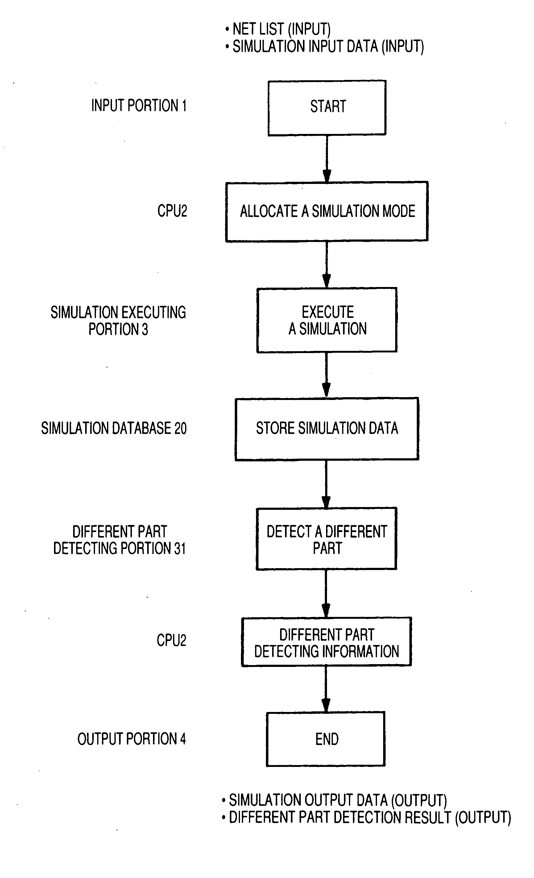
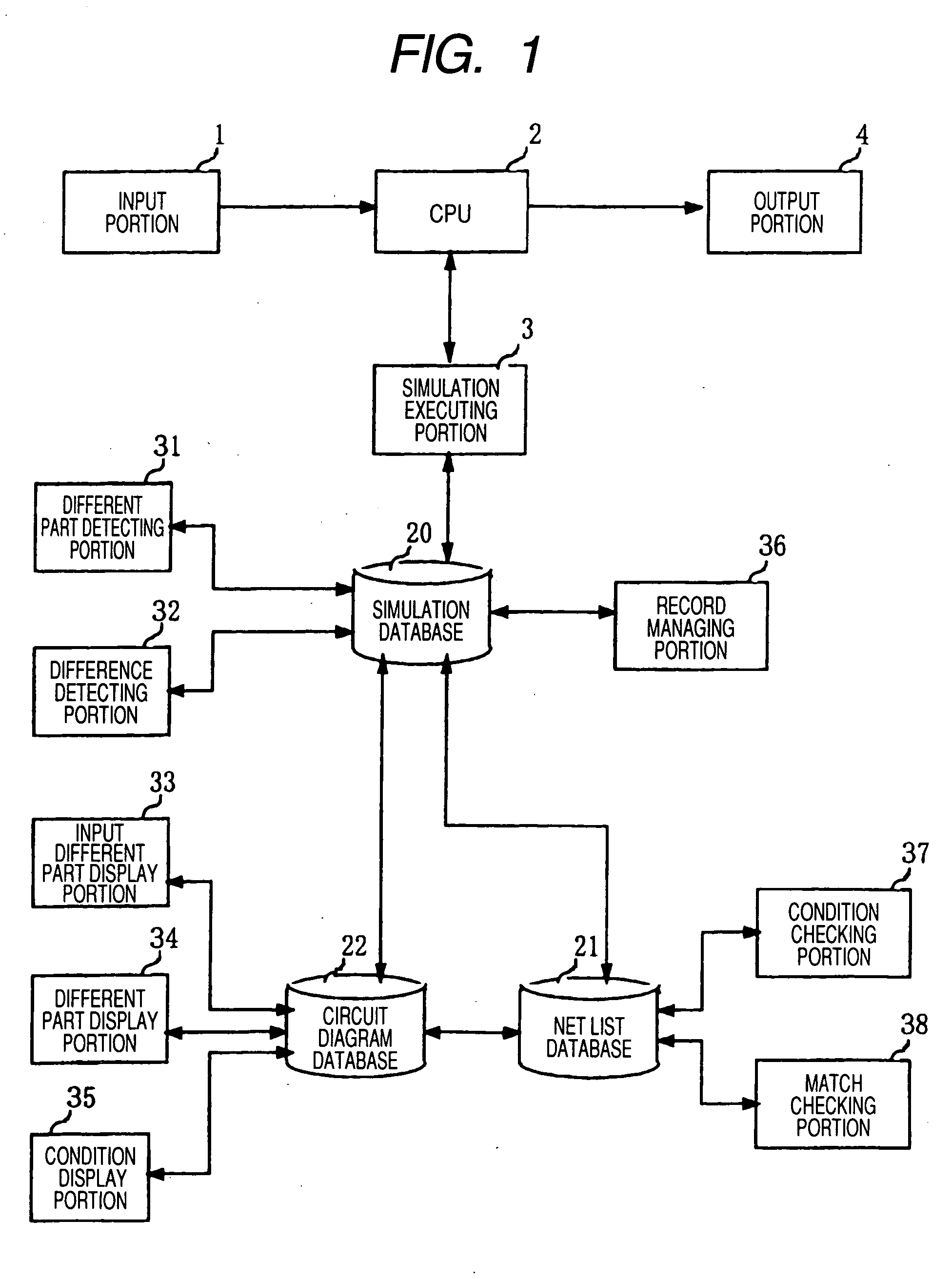
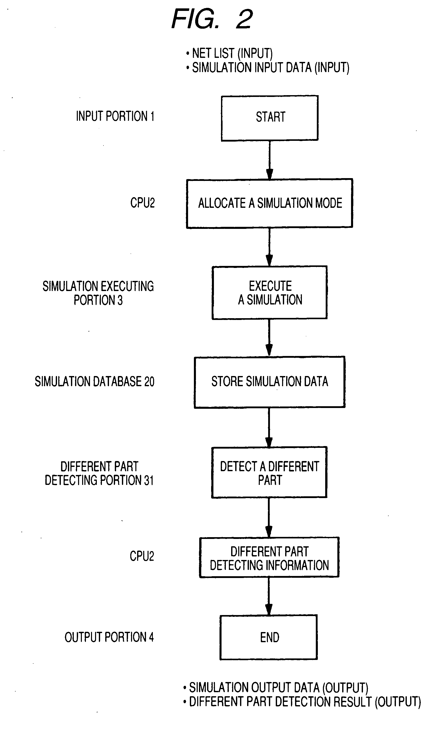
[0073] An embodiment of the invention will be described below with reference to the drawings. FIG. 1 is a block diagram showing the structure of a semiconductor designing apparatus according to an embodiment of the invention. In FIG. 1, 1 denotes an input portion, 2 denotes a CPU, 3 denotes a simulation executing portion, and 4 denotes an output portion, and these have the same structures as those in FIG. 22.

[0074] In FIG. 1, furthermore, 20 denotes a simulation database, 21 denotes a net list database, 22 denotes a circuit diagram database, 31 denotes a different part detecting portion, 32 denotes a difference detecting portion, 33 denotes an input different part display portion, 34 denotes a different part display portion, 35 denotes a condition display portion, 36 denotes a record managing portion, 37 denotes a condition checking portion, and 38 denotes a match checking portion.

[0075] The simulation database 20 stores the processing result of a simulation, the net list database...


PUM


Abstract

There are provided a different part detecting portion for detecting the different part of the result of a simulation, a difference detecting portion for detecting a difference in the result of a simulation, an input different part display portion for displaying any of circuits having different simulation modes which has a difference, a different part display portion for displaying a circuit having a difference in the result of a simulation, a condition display portion for displaying, on a circuit diagram, an option to be used in a simulation, a record managing portion for managing the execution history of the result of a simulation, a condition checking portion for ascertaining whether or not a condition is accurately set in each circuit in the execution of a simulation, and a match checking portion for confirming the non-coincidence of the names and numbers of pins between the simulation modes.

Description

BACKGROUND OF THE INVENTION [0001] 1. Field of the Invention [0002] The present invention relates to a semiconductor designing apparatus to be used for designing a semiconductor circuit. [0003] 2. Description of the Related Art [0004] In the case in which a memory circuit or an analog circuit of a semiconductor is to be designed, heretofore, a function is verified digitally by utilizing a C language at the early stage of a design phase and an analog circuit simulation is carried out for each block by using SPICE when the design phase progresses. Thus, the design is verified. [0005] In recent years, moreover, an analog / digital mixing simulator has been set to have a practical level, and analog and digital simulations can be mixed and carried out (for example, see Analog / Digital Mixing Simulator, Nikkei Electronics (10-14) Special issue, Nikkei BP Co., Ltd., Oct. 14, 1996, P. 120). [0006] Consequently, a simulation mode to be used for each block corresponding to the progress of the de...

Claims


Application Information

Patent Timeline
Patent Type & Authority Applications(United States)
IPC IPC(8): G06F17/50
CPCG06F17/5022G06F17/5036G06F30/33G06F30/367
Inventor ISHIYAMA, YASUHIRO
Owner PANASONIC CORP
Why Eureka
Try Eureka