Side-emitting solid-state semiconductor light emitting device

Inactive Publication Date: 2006-09-21
UNITY OPTO TECH CO LTD +1
View PDF3 Cites 27 Cited by
  • Summary
  • Abstract
  • Description
  • Claims
  • Application Information

AI Technical Summary

Benefits of technology

[0005] The main object of the present invention is to provide an improved structure of a side-emitting solid-state semiconductor light emitting device for redirecting the light emitted from a light emitting diode by combining the light emitting diode with

Problems solved by technology

The aforementioned method only changes the angle and the mounting position of the light emitting diode so as to provide the user with the required light emittin

Method used


Image

  • Side-emitting solid-state semiconductor light emitting device
  • Side-emitting solid-state semiconductor light emitting device
  • Side-emitting solid-state semiconductor light emitting device

Examples


Example

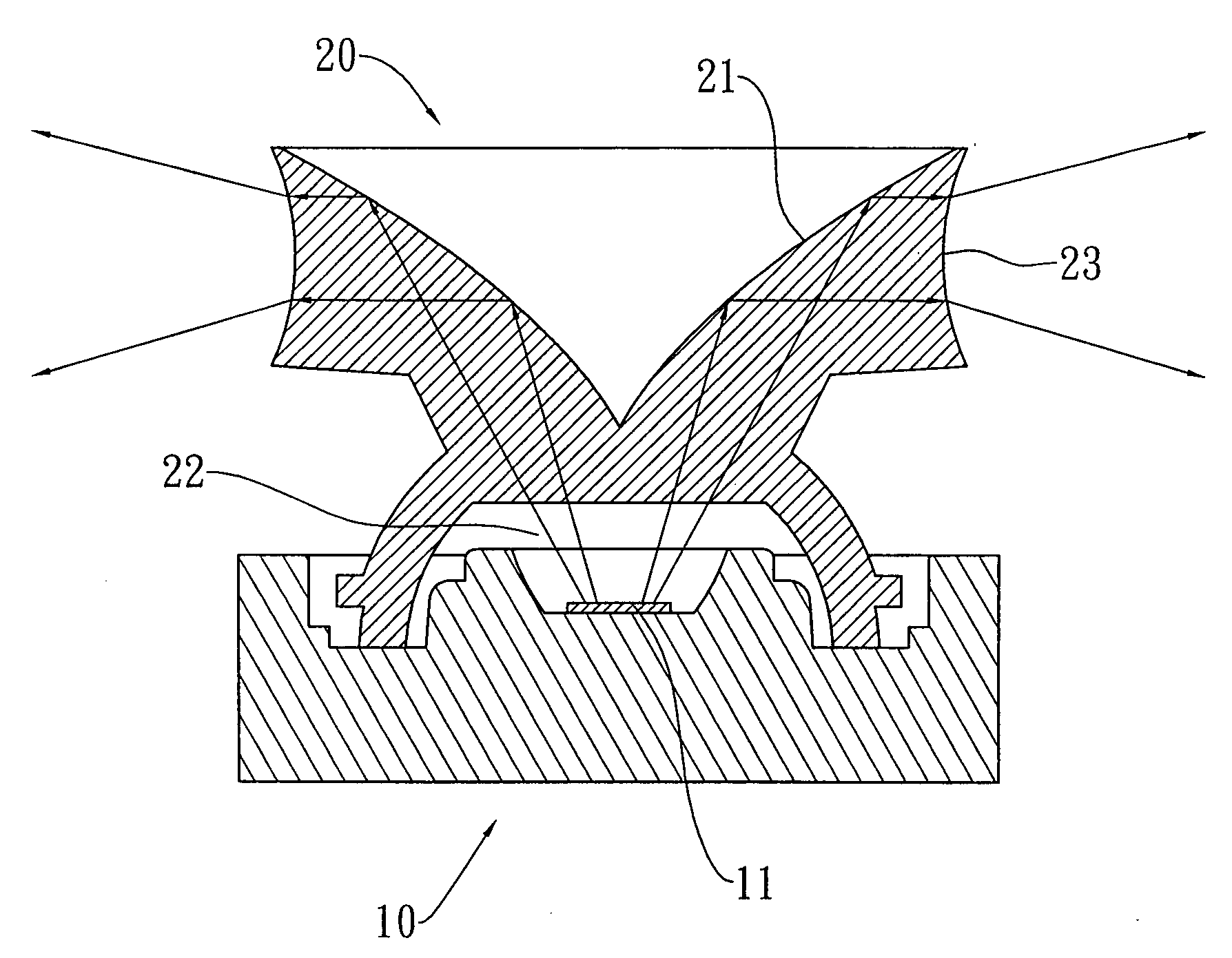
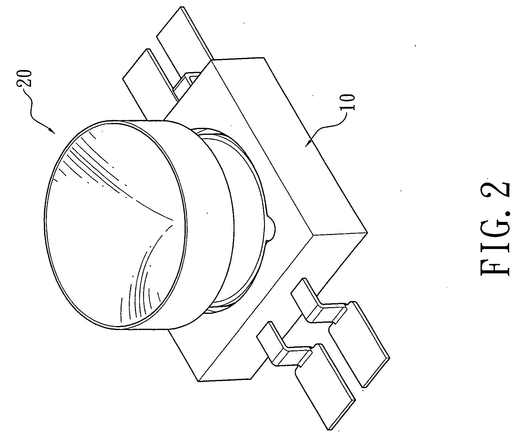
[0015] Referring to FIG. 2 and FIG. 3 simultaneously, a side-emitting solid-state semiconductor light emitting device of the present invention comprises a light emitting diode package 10 and a lens 20, wherein the lens 20 covers a chip 11 of the light emitting diode package 10 from top to toe to complete the assembly. The lens 20 is roughly a cylinder having a concave holding room 22 on its bottom to hold the chip 11 of the light emitting diode package 10, and the top of the lens 20 is concaved gradually from the periphery to the center to form a concave surface and this concave surface is designed to be a reflecting part 21. The outer periphery of the top of the lens 20 (i.e. the concave surface) constitutes a projecting part 23, wherein the projecting part 23 is a flat surface for emitting the light outward uniformly. Accordingly, the light emitted upwardly from the chip 11 is reflected by the reflecting part 21 of the lens 20 and the reflected light is side-emitted outward unifor...


PUM


Abstract

A side-emitting solid-state semiconductor light emitting device (light emitting diode) comprises a light emitting diode package and a lens, wherein the lens is mounted on the front surface of the light emitting diode package to receive the light emitted from the light emitting diode and redirect the received light by use of a reflecting part to project the light on the peripheral surface of the light emitting diode package. This peripheral surface is designed to provide various changes and the side-emitting light is changed according to the changes of the peripheral surface.

Description

FIELD OF THE INVENTION [0001] The present invention relates to an improved structure of a side-emitting solid-state semiconductor light emitting device, and more particularly to a structure for redirecting the path of the light emitted from the light emitting diode by use of the lens and the redirected light is further changed-according to the changes of the periphery of the lens, and this structure is suitable for the marketplaces, all kinds of advertising billboards, backlight sources, or the likes. BACKGROUND OF THE INVENTION [0002] The light emitted from a conventional light emitting diode is the forward-emitting light and the light emitting diode is coupled with a printed circuit board to assign the emitting direction of the light. The simplest method is to change the mounting position of the printed circuit board. For example, the printed circuit board is mounted vertically in the machine to emit the side-emitting light or the printed circuit board is mounted on the top of the...

Claims


Application Information

Patent Timeline
IPC IPC(8): H01L29/18
CPCH01L33/58H01L33/60G02B19/0071G02B19/0028G02B19/0061
Inventor CHIN, YUAN-CHENGLI, HUNG-CHIH
Owner UNITY OPTO TECH CO LTD
Why Eureka
Try Eureka