Silicon wafer heat treatment jig, and silicon wafer heat treatment method

Active Publication Date: 2006-09-21
SUMCO CORP
View PDF3 Cites 7 Cited by
  • Summary
  • Abstract
  • Description
  • Claims
  • Application Information

AI Technical Summary

Benefits of technology

[0017] In a heat treatment method of the invention, by setting the support points to form an angle of 120° about the center and to be positioned within a region where a radial distance from the center is defined by 85 to 99.5% of the wafer radius, it is possible to control lengths of slip dislocations grown from the reverse surface of the wafer caused by contact with the support projections, so that the dislocation lengths are short enough not to affect a device formation region of the wafer surface.
[0018] By this method, generation of slip dislocations in the device formation region is reduced and a reduction in wafer yield can be prevented.
[0021] In the heat treatment jig of the invention, support projections are provided on the upside of three support arms comprised of a first, a second, and a third arm protruding towards a center intervening spacing from the support frame so that the arms forming an angle of 120° with each other. The positions of the support projections can be preset so that each projection is positioned in the same circle about the center, within a region where a radial distance from the center is defined by 85 to 99.5% of the wafer radius. Accordingly, all the supporting positions of a silicon wafer form an angle of 120° about the center and are positioned within a region where a radial distance from the center is defined by 85 to 99.5% of the wafer radius, thereby lengths of slip dislocations caused by contacts with support projections can be controlled to sufficiently short lengths that do not affect the device formation region of the wafer surface.
[0022] In the invention, by enabling presetting of the fixing position of the support projection on the support arm and fixing the projection to that position, the support position of the wafer can be preset in accordance with the diameter, thickness, hardness / stress properties, thermal properties or the like of the wafer so that the length of slip dislocations caused by contact with the support projections can be controlled to sufficiently short lengths that do not affect the device formation region of the surface of the silicon wafer.

Problems solved by technology

However, in the heat treatment of wafers horizontally supported during the treatment, there has been a problem of yield reduction caused by generation of slip dislocations.
It is considered that, since supported portions of the wafer are pressed by their own weight, sliding friction between the wafer and the projections is caused by warping of the wafer during the heat treatment or by a difference in heat expansion, strain occurs in a portion of concentrated weight, and therefore each portion supported by support projections generates slip dislocations.

Method used


Image

  • Silicon wafer heat treatment jig, and silicon wafer heat treatment method
  • Silicon wafer heat treatment jig, and silicon wafer heat treatment method
  • Silicon wafer heat treatment jig, and silicon wafer heat treatment method

Examples


example 1

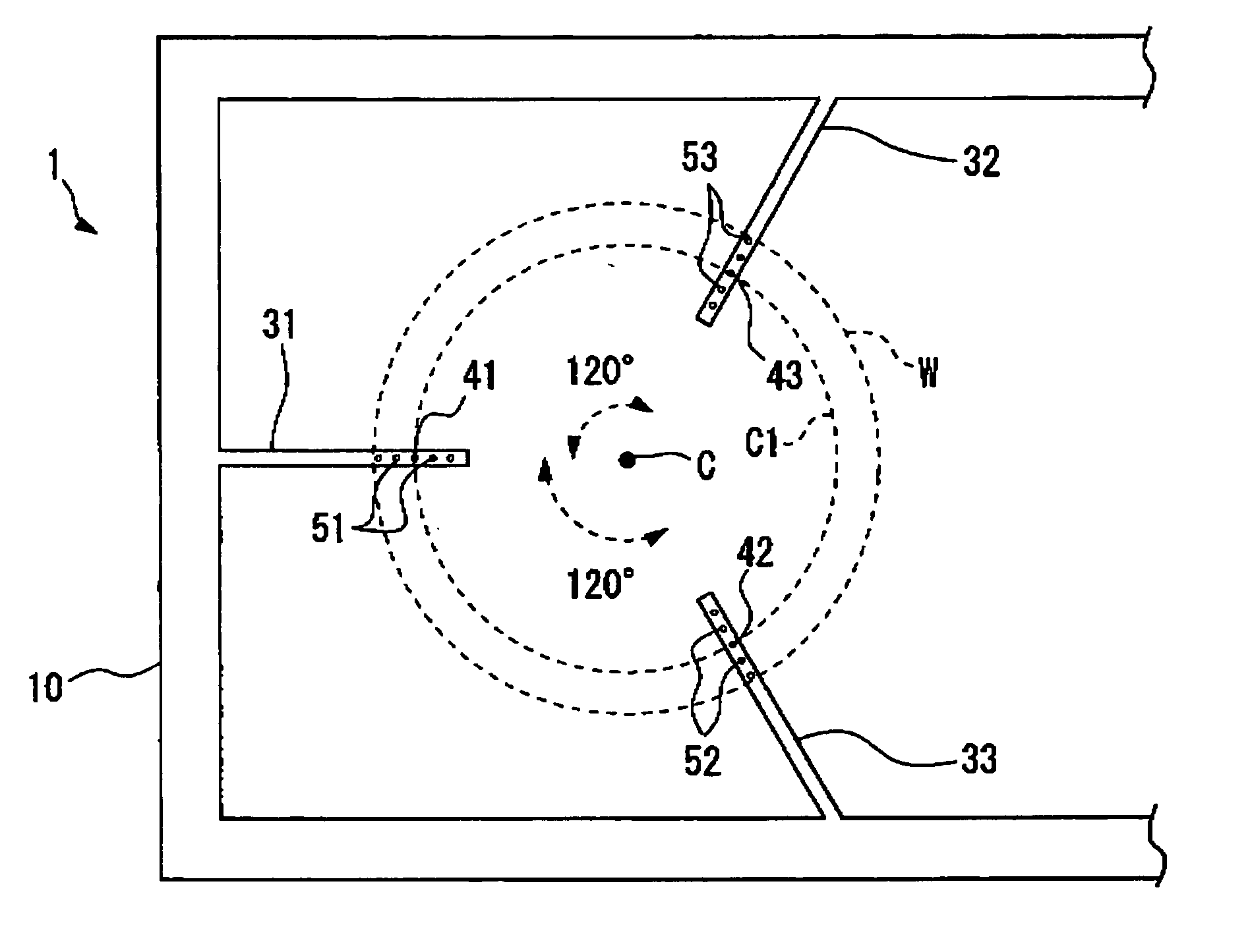
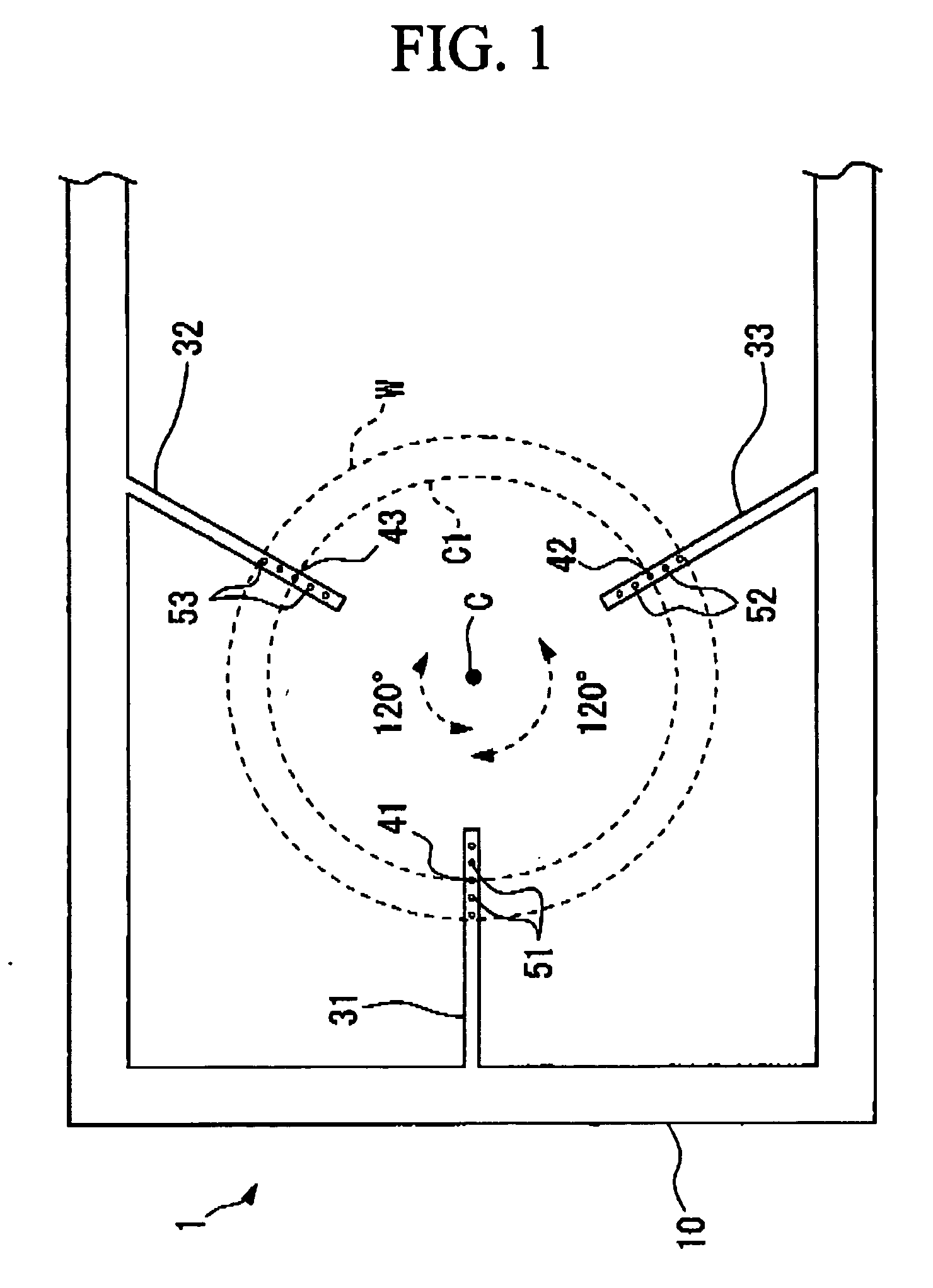
[0050] Silicon wafers lacking an orientation flat (notch-type silicon wafers) of 200 mm in diameter, 0.725 mm in thickness are prepared.

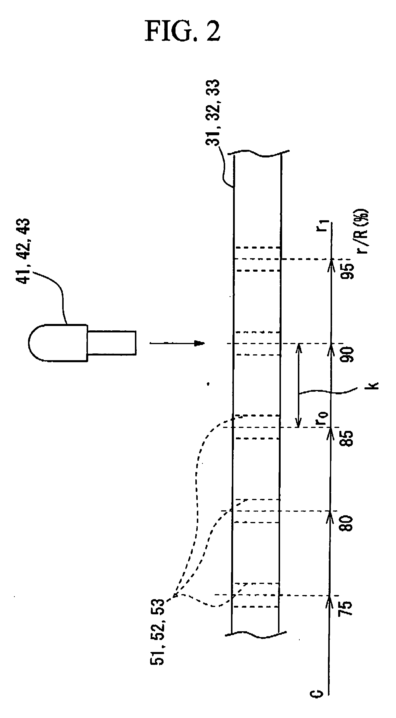
[0051] The support projections 41, 42, 43 shown in FIGS. 1 and 3 are positioned around the same circle of radius r and are concentric with the wafer W about the center C. Where the wafer radius is termed R, the positions are controlled so that the r / R value was varied at every 5% interval, from 65% to 90%, and was 97%. The silicon wafer W was mounted on the support projections with the above described arrangement and was supported horizontally. The heat treatment jig 1 being mounted with the silicon wafer was transferred to the heat treatment furnace 20 shown in FIG. 4, and the wafer W was heat-treated for 10 seconds at a furnace temperature of 1250° C.


PUM

PropertyMeasurementUnit
Fractionaaaaaaaaaa
Angleaaaaaaaaaa
Distanceaaaaaaaaaa

Abstract

In this heat treatment jig and method for silicon wafers, a silicon wafer is heat-treated while being mounted on support projections provided on three support arms, having an intervening spacing, protruding from a support frame towards the center. At that time, all the support projections under the silicon wafer are positioned on a same circle within a region where a radial distance from the center is defined by 85 to 99.5% of the wafer radius, and the support arms form an angle of 120° with each other about the center. With this jig and method, free depth of a dislocation generated from a pin position can be controlled deeper than a device formation region, and a widest slip-free region where the surface is free from slip dislocation is obtained.

Description

TECHNICAL FIELD [0001] The present invention relates to heat treatment jig for a wafer and heat treatment method for a wafer, specifically relates to a technology suitably used in RTA or the like. [0002] Priority is claimed on Japanese Patent Application No. 2003-097365 filed 31 March, 2003, the content of which is incorporated herein by reference. BACKGROUND ART [0003] Conventionally, a rapid thermal annealer (RTA) is well known as a heat treatment apparatus for rapid heating and rapid cooling of a silicon wafer. As described in FIG. 3(a) of Patent Reference 1, a ring-shaped wafer holder 100 is mounted within a furnace of the rapid thermal annealer in order to maintain a horizontal orientation of the wafer. [0004] As shown in Patent Reference 2, in another well known type of wafer holder, a wafer is supported by a plurality of points. [0005] However, in the heat treatment of wafers horizontally supported during the treatment, there has been a problem of yield reduction caused by ge...

Claims


Application Information

Patent Timeline
IPC IPC(8): B23B31/28B29C71/00H01L21/00H01L21/683H01L21/26H01L21/324
CPCF27B17/0025F27D5/0037Y10T279/23H01L21/67109H01L21/324H01L21/68
Inventor NAKADA, YOSHINOBUSHIRAKI, HIROYUKIHASEGAWA, TAKESHI
Owner SUMCO CORP
Why Eureka
Try Eureka