Mode size converter for a planar waveguide

Inactive Publication Date: 2005-04-26
DEMARAY
View PDF10 Cites 74 Cited by
  • Summary
  • Abstract
  • Description
  • Claims
  • Application Information

AI Technical Summary

Benefits of technology

[0010]In accordance with the present invention, a smooth waveguide taper is presented. A smooth waveguide taper can be produced as an out-of-plane taper during deposition of the film by a shadow-mask deposition. A shadow mask is placed over the substrate in a PVD reactor during deposition. The resulting taper can be monotonically variable in thickness as well as atomic like in smoothness.

Problems solved by technology

In practice however, it is difficult to change the dimensions of a planar wave guide without loss due to roughness or to non-uniform changes in the wave guide.
In particular, sufficiently slowly varying dimensions with a sufficiently smooth surface, so that the light is efficiently converted in its modal properties, without scattering or loss due to roughness or to non-uniform changes in the dimensions or index of the wave guide is very hard to achieve, particularly for high contrast or refractory wave guide materials.
However, it is difficult to achieve sufficiently uniform results for a portion of a film or wave guide tapered over a few mm to a few cm regions across, for instance, a production silicon wafer having dimensions of 100 to 300 mm.

Method used


Image

  • Mode size converter for a planar waveguide
  • Mode size converter for a planar waveguide
  • Mode size converter for a planar waveguide

Examples


Embodiment Construction

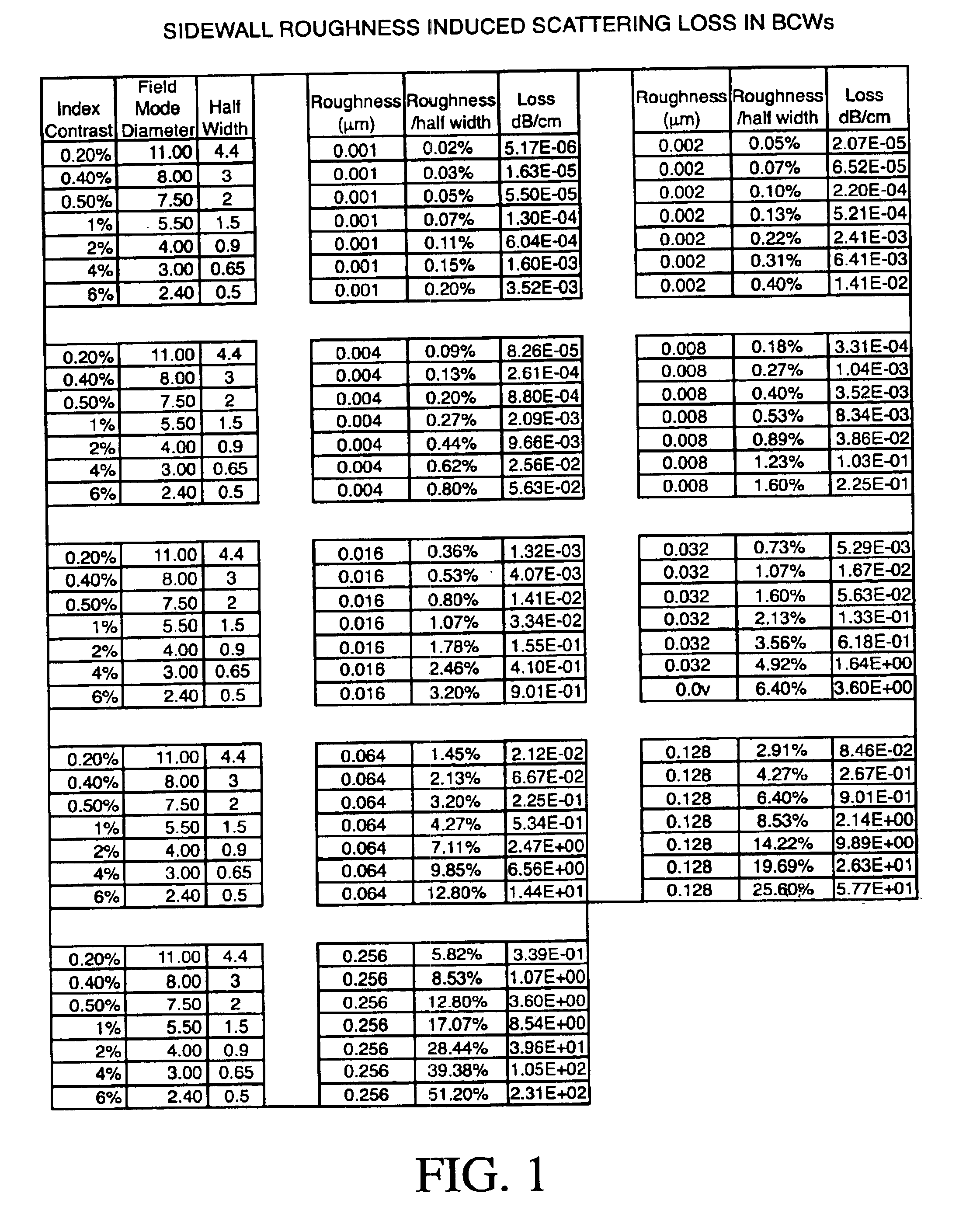
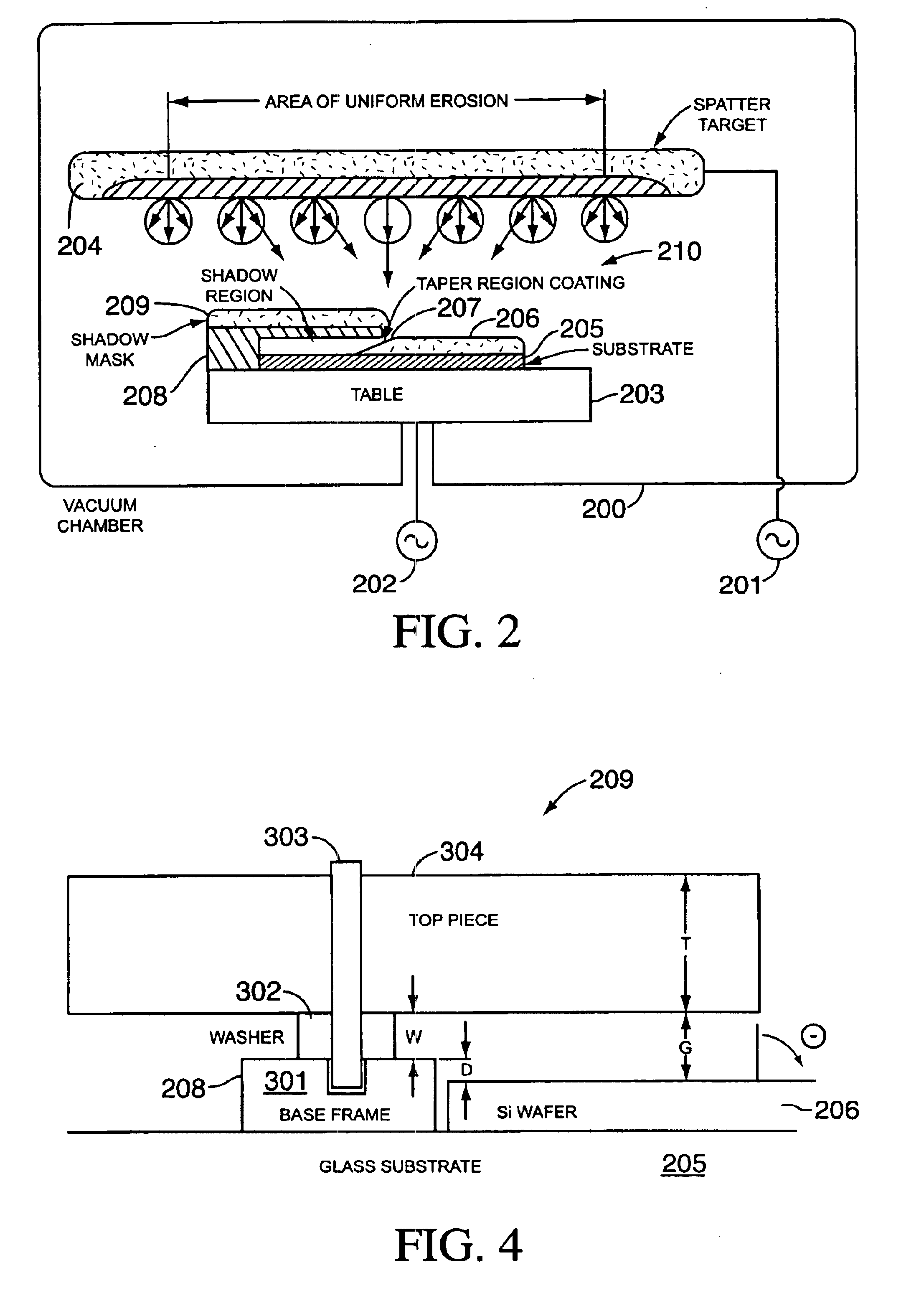
[0034]RF sputtering of oxide films is discussed in application Ser. No. 09 / 903,050 (the '050 application) by Demaray et al., entitled “Planar Optical Devices and Methods for Their Manufacture,” assigned to the same assignee as is the present invention, herein incorporated by reference in its entirety. Depositions by biased pulse-DC sputtering are described in U.S. application Ser. No. 10 / 101,863 (the '863 application), herein incorporated by reference in its entirety. Further, targets that can be utilized in a reactor according to the present invention are discussed in U.S. application Ser. No. 10 / 101,341 (the '341 application), filed concurrently with the present disclosure, assigned to the same assignee as is the present invention, herein incorporated by reference in its entirety. A gain-flattened amplifier formed of films deposited according to the present invention are described in U.S. application Ser. No. 10 / 101,493 (the '493 application) filed concurrently with the present di...


PUM


Abstract

A process for forming a mode size converter with an out-of-plane taper formed during deposition with a shadow mask is disclosed. Mode-size converters according to the present invention can have any number of configurations. Measured coupling efficiencies for waveguides with mode size converters according to the present invention show marked improvement.

Description

BACKGROUND[0001]1. Field of the Invention[0002]The present invention relates to optical coupling into a planar waveguide and, in particular, to a mode size converter for coupling light into and out of a planar waveguide and to efficiently transform guided light within continuous waveguide structures.[0003]2. Discussion of Related Art[0004]The increasing prevalence of fiber optic communications systems has created an unprecedented demand for devices for processing optical signals. Planar devices such as optical waveguides, couplers, splitters, and amplifiers, fabricated on planar substrates, like those commonly used for integrated circuits, and configured to receive and process signals from optical fibers are highly desirable. Such devices hold promise for integrated optical and electronic signal processing on a single semiconductor-like substance.[0005]The basic design of planar optical waveguides and amplifiers is well known, as described, for example, in U.S. Pat. Nos. 5,119,460 a...

Claims


Application Information

Patent Timeline
IPC IPC(8): C23C14/04G02B6/13G02B6/132G02B6/122G02B6/12
CPCC23C14/044G02B6/132G02B6/1228G02B2006/12195
Inventor PAN, TAODEMARAY, RICHARD E.CHEN, YUXIE, YONG JINPETHE, RAJIV
Owner DEMARAY
Why Eureka
Try Eureka