Active matrix liquid crystal display device

a liquid crystal display and active matrix technology, applied in the field of active matrix liquid crystal display devices, can solve the problems of inferior display characteristics, deterioration of viewing angle characteristics, and affecting the appearance of objects, so as to improve brightness and contrast, increase the effective area of pixel electrodes and common electrodes, and improve the effect of aperture ratio

Active Publication Date: 2006-09-28
HANNSTAR DISPLAY CORPORATION
View PDF3 Cites 10 Cited by
  • Summary
  • Abstract
  • Description
  • Claims
  • Application Information

AI Technical Summary

Benefits of technology

[0017] A first advantage of the present invention is that it is possible to increase aperture ratio and to improve brightness and contrast compared with the IPS mode LCD device of the related art. The reason for the above is that, since the pixel electrodes and the common electrodes for generating a lateral electric field are formed on the both side walls of the convex part formed along the data wiring, effective areas of the pixel electrodes and the common electrodes can be increased. Thus, it is no longer required to form comb-teeth-shaped electrodes crossing an aperture of a pixel region. Specifically, the effective areas of the pixel electrodes and the common electrodes can be increased while suppressing an increase in an occupied area in a planar direction on the substrate.
[0018] Moreover, a second advantage of the present invention is that viewing angle characteristics can be improved compared with the IPS mode LCD device of

Problems solved by technology

Thus, the viewing angle characteristics may be deteriorated.
Thus, inferior dis

Method used


Image

  • Active matrix liquid crystal display device
  • Active matrix liquid crystal display device
  • Active matrix liquid crystal display device

Examples


Embodiment Construction

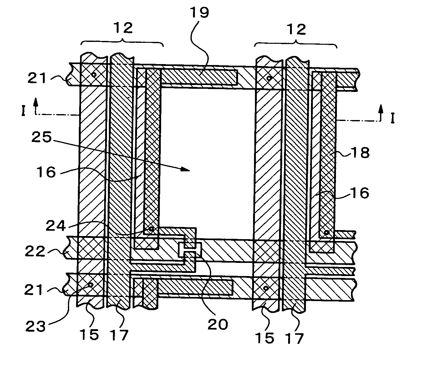
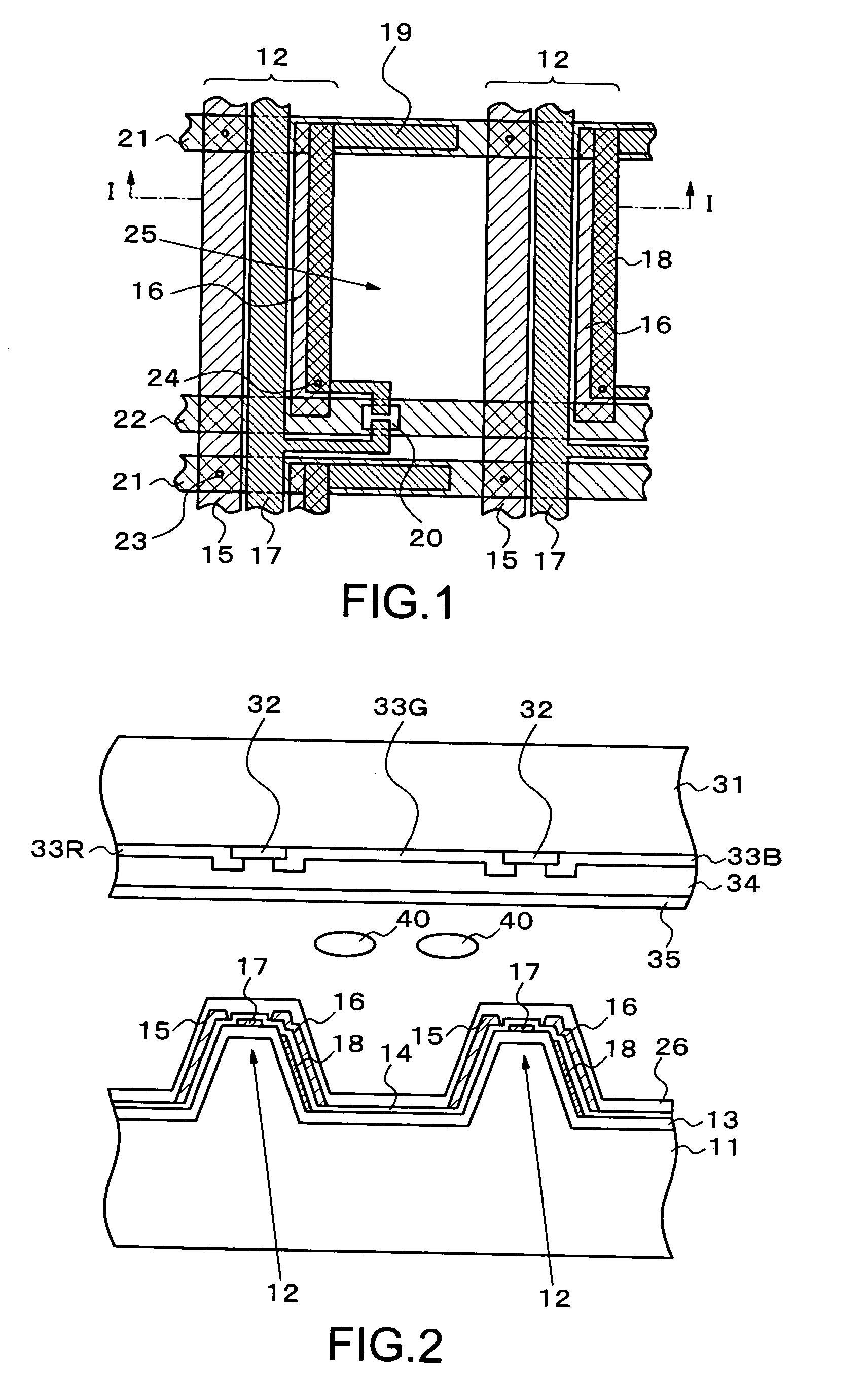
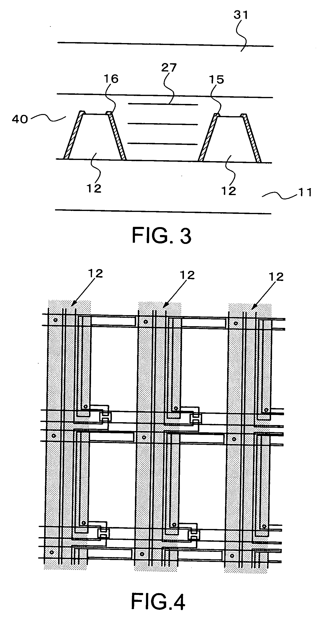
[0030] According to an embodiment of the present invention, convex parts, each having a trapezoidal cross section or the like, are formed so as to overlap with at least a region where data wirings are formed on a TFT substrate included in an active matrix LCD device. A pixel electrode is formed in a region including at least a part of one of side walls of the convex part. Moreover, a common electrode is formed in a region including at least a part of the other side wall. Between the convex parts adjacent to each other, the pixel electrodes and the common electrodes are set to face each other. In the structure described above, since effective areas of the pixel electrodes and the common electrodes can be increased, it is no longer required to form comb-teeth-shaped electrodes crossing an aperture of a pixel region. Thus, aperture ratio can be increased compared with an IPS mode LCD device of the related art. Moreover, since the pixel electrodes and the common electrodes can be set to...


PUM

PropertyMeasurementUnit
Angleaaaaaaaaaa

Abstract

In a region where data wirings are formed on a TFT substrate, convex parts, each having a trapezoidal cross section or the like, are formed. A pixel electrode is formed on one of side faces of the convex part, and a common electrode is formed on the other side face. Furthermore, the pixel electrodes and the common electrodes are set to face each other between the convex parts adjacent to each other.

Description

BACKGROUND OF THE INVENTION [0001] 1. Field of the Invention [0002] The present invention relates to an active matrix liquid crystal display device, and more particularly relates to an in-plane switching mode active matrix liquid crystal display device. [0003] 2. Description of the Related Art [0004] In recent years, an active matrix liquid crystal display (LCD) device using a thin film transistor (TFT) as a switching element of a pixel has been widely used. Operation modes of the LCD device described above include: a twisted nematic (TN) mode of rotating liquid crystal molecules in a direction perpendicular to a glass substrate; and a lateral electric field mode of rotating liquid crystal molecules in a direction parallel to a glass substrate. The lateral electric field mode is also called an in-plane switching (IPS) mode. [0005] As shown in FIG. 8 or FIG. 9, in an IPS mode LCD device, normally, pixel electrodes 51 and common electrodes 52 are alternately formed so as to be paralle...

Claims


Application Information

Patent Timeline
IPC IPC(8): G02F1/1343
CPCG02F1/134363G02F1/136286G02F2001/133776G02F2001/136295G02F2201/40G02F1/133776G02F1/136295D06B1/02D06B3/10D06B3/36D06P5/15
Inventor ITO, HIDEKI
Owner HANNSTAR DISPLAY CORPORATION
Why Eureka
Try Eureka