Circuit for data bit inversion

a data bit and circuit technology, applied in the field of circuit units for data bit inversion, can solve problems such as increasing inductive and capacitive couplings, increasing data falsification instances, and becoming more difficult to transfer data from memory modules to controllers

Inactive Publication Date: 2006-09-28
POLARIS INNOVATIONS
View PDF3 Cites 11 Cited by
  • Summary
  • Abstract
  • Description
  • Claims
  • Application Information

AI Technical Summary

Benefits of technology

[0039]FIG. 6, as discussed above, is a block diagram of a decoder within the conventional

Problems solved by technology

The inductive and capacitive couplings increase because of the increasing operating frequency, and so instances of data falsification occur.
With increasing operating frequency, it becomes ever more difficult to transfer the data from the memory module to the controller.
The noise on the data lines of the data bus constitutes one limitation here.
The noise limits the validity period of the data and reduces the so-called data eye size.
The more switching processes and/or data transfers that occur on the dat

Method used


Image

  • Circuit for data bit inversion
  • Circuit for data bit inversion
  • Circuit for data bit inversion

Examples


Embodiment Construction

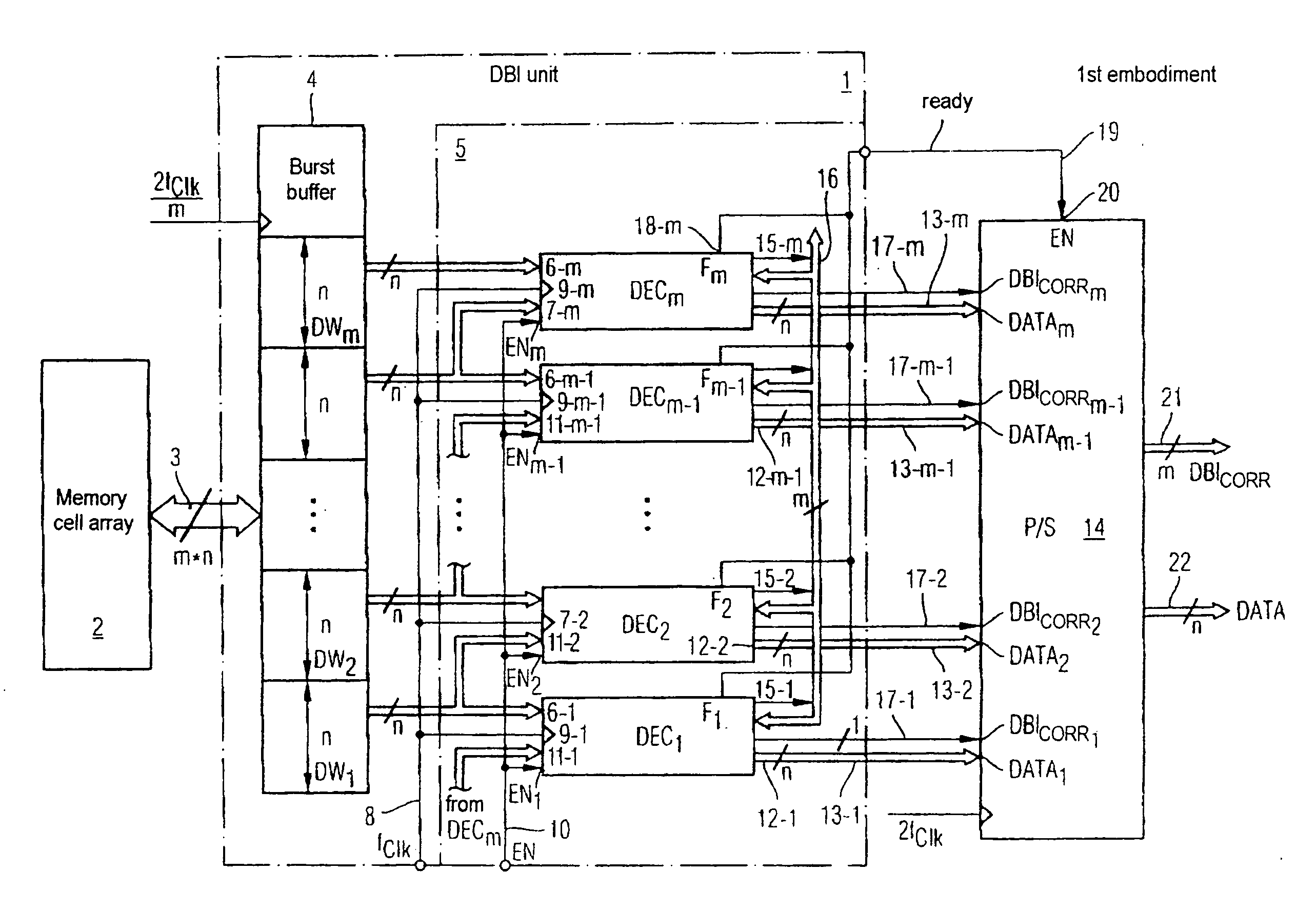
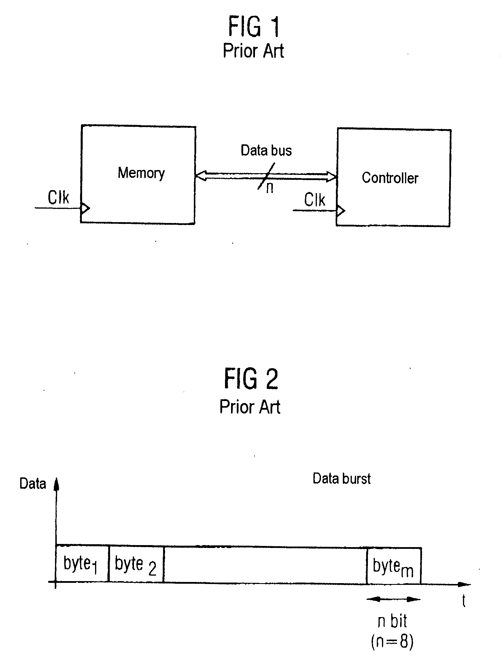
[0049]FIG. 7 illustrates a first embodiment of the circuit unit 1 according to the invention for data bit inversion of a data burst which has been read from a memory module. The circuit unit 1 according to the invention is integrated within the memory module and forms part of the read signal path. The memory module contains a memory cell array 2 having a multiplicity of memory cells for storing data bits. An internal data bus 3 is used to buffer all the data bits of a data burst which is to be read in a burst buffer 4 of the circuit unit 1. If the data burst consists of m data words each containing n data bits, m-n data bits are simultaneously written to the burst buffer 4.

[0050] The circuit unit 1 contains a decoder unit 5 which consists of a number of decoders 5-i connected up in parallel. For each data word DWi, an associated decoder 5-i is provided within the decoder unit 5. Each decoder 5-i respectively compares the associated data word DWi, present at it, of the buffered data...


PUM


Abstract

An electric circuit for inverting a data bit of a data burst read out from a memory module comprises a buffer for buffering a data burst being comprised of at least two data words, a decoder device comprised of at least two parallel-connected decoders, each comparing bitwise and simultaneously two neighbouring data words of the data words buffered in the buffer and generating an inversion flag, if the number of different data bits of the two neighbouring data words exceeds half the number of data bits of a data word, a correction device for generating a corrected inversion flag for a specific decoder of the decoders by inverting or not inverting the inversion flag of the specific decoder dependent on the inversion flag generated by the specific decoder and the inversion flags generated by the remaining of the decoders, and an inversion device comprised of a plurality of inverters, each inverting or not inverting a present of the data words of an associated of the decoders dependent on the corrected inversion flag of the associated decoder.

Description

BACKGROUND OF THE INVENTION [0001] 1. Field of the Invention [0002] The invention relates to a circuit unit for data bit inversion of a data burst read out from a memory module, in particular for DDR-SDRAM (Double Data Rate Synchronous Dynamic Random Access Memories). [0003] 2. Description of the Prior Art [0004]FIG. 1 shows a computer system according to the prior art in which a memory chip and a controller chip exchange data via a common data bus. The increasing speed of computer processors and / or controllers requires a correspondingly higher speed in the case of instances of memory access and / or faster memory modules. The memory module and the processor are clocked via a clock signal CLK. [0005] Various generations of RAM memories have been developed whose access rate has risen continuously. The time intervals in which new data read out from the memory cell array or to be written are present at the data inputs / outputs of the corresponding memory module have been shortening contin...

Claims


Application Information

Patent Timeline
IPC IPC(8): G11C7/00
CPCG06F11/08G11C7/1006
Inventor DIETRICH, STEFAN
Owner POLARIS INNOVATIONS
Why Eureka
Try Eureka