Semiconductor device with a high-k gate dielectric and a metal gate electrode

a technology of metal gate electrodes and semiconductor devices, which is applied in the direction of semiconductor devices, electrical devices, transistors, etc., can solve the problems of high-k material, deformation of mobility, and inability to meet the requirements of high-k materials,

Inactive Publication Date: 2006-10-05
TAHOE RES LTD
View PDF37 Cites 17 Cited by
  • Summary
  • Abstract
  • Description
  • Claims
  • Application Information

AI Technical Summary

Problems solved by technology

MOS field-effect transistors with very thin silicon dioxide based gate dielectrics may experience unacceptable off-state leakage.
Replacing low-k silicon dioxide with a high-k material may, however, degrade mobility.

Method used


Image

  • Semiconductor device with a high-k gate dielectric and a metal gate electrode
  • Semiconductor device with a high-k gate dielectric and a metal gate electrode

Examples


Embodiment Construction

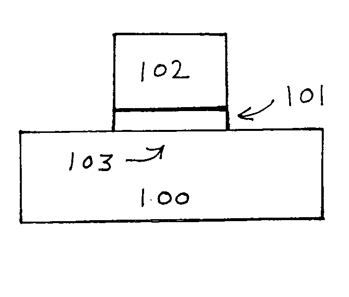
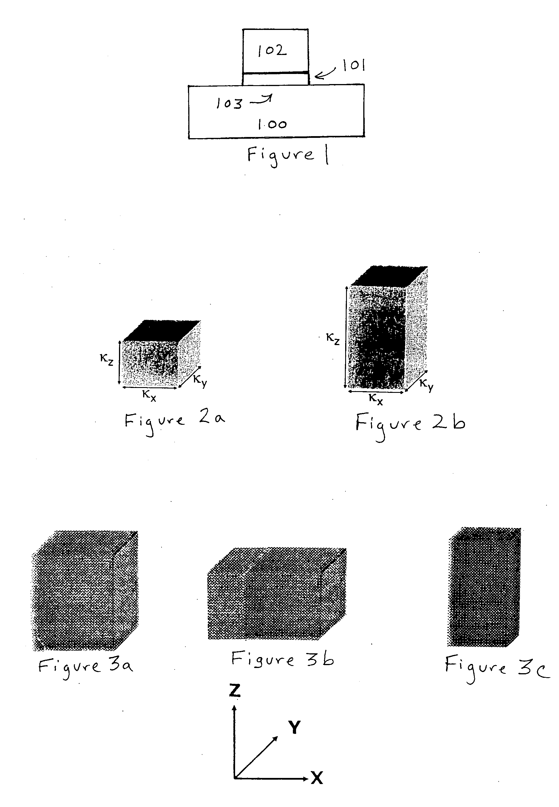
[0008] A semiconductor device is described. That semiconductor device comprises a high-k gate dielectric layer that is formed over a channel that is positioned within a substrate, and a metal gate electrode that is formed on the high-k gate dielectric layer. The high-k gate dielectric layer has off-state leakage characteristics that are superior to those of a silicon dioxide based gate dielectric, and on-state mobility characteristics that are superior to those of a high-k gate dielectric that comprises an isotropic material.

[0009] In the following description, a number of details are set forth to provide a thorough understanding of the present invention. It will be apparent to those skilled in the art, however, that the invention may be practiced in many ways other than those expressly described here. The invention is thus not limited by the specific details disclosed below.

[0010] FIGS. 1 represents a cross-section of the semiconductor device of the present invention. In that sem...


PUM


Abstract

A semiconductor device is described. That semiconductor device comprises a high-k gate dielectric layer that is formed over a channel that is positioned within a substrate, and a metal gate electrode that is formed on the high-k gate dielectric layer. The high-k gate dielectric layer has off-state leakage characteristics that are superior to those of a silicon dioxide based gate dielectric, and on-state mobility characteristics that are superior to those of a high-k gate dielectric that comprises an isotropic material.

Description

FIELD OF THE INVENTION [0001] The present invention relates to semiconductor devices, in particular, those with high-k gate dielectrics and metal gate electrodes. BACKGROUND OF THE INVENTION [0002] MOS field-effect transistors with very thin silicon dioxide based gate dielectrics may experience unacceptable off-state leakage. Forming the gate dielectric from certain high-k dielectric materials can reduce gate leakage. Replacing low-k silicon dioxide with a high-k material may, however, degrade mobility. [0003] Accordingly, there is a need for a semiconductor device with a high-k gate dielectric that has both acceptable off-state leakage and on-state mobility characteristics. The present invention discloses such a semiconductor device.BRIEF DESCRIPTION OF THE DRAWINGS [0004]FIG. 1 represents a cross-section of the semiconductor device of the present invention. [0005]FIGS. 2a and 2b graphically illustrate the relative dielectric constants for isotropic and anisotropic materials in ver...

Claims


Application Information

Patent Timeline
Patent Type & Authority Applications(United States)
IPC IPC(8): H01L29/94
CPCH01L21/28194H01L29/495H01L29/7843H01L29/516H01L29/517H01L29/4966
Inventor METZ, MATTHEW V.DATTA, SUMANDOCZY, MARK L.KAVALIEROS, JACKBRASK, JUSTIN K.DOYLE, BRIAN S.RADOSAVLJEVIC, MARKOCHAU, ROBERT S.
Owner TAHOE RES LTD
Why Eureka
Try Eureka