
Distributed constant circuit and impedance adjustment method

Inactive Publication Date: 2006-10-05
TDK CORPARATION
View PDF3 Cites 1 Cited by
  • Summary
  • Abstract
  • Description
  • Claims
  • Application Information

AI Technical Summary

Benefits of technology

[0011] To solve the above-described problems, an object of the present invention is to provide a distributed constant circuit capable of adjusting the impedance matching between the conductor line such as the micro strip line and an electronic device easily, disposed in a small area.
[0014] As a consequence, the present invention enables to adjust the impedance matching between the characteristic impedance of the conductor line and the load impedance or drive impedance of an electronic device easily by moving the adjustment tab into a contact with the conductor line even if there is only a small area on the substrate. Further, the adjustment tab can be removed, so that the characteristic of the conductor line can be provided only by removing it.
[0016] The inventor has clarified that electric field is concentrated on the corners of the adjustment tab by simulation. If electric field is concentrated, a slight change of position of the adjustment tab fluctuates the impedance characteristic largely. If the corners are chamfered, concentration of electric field can be prevented so as to adjust the impedance matching easily.
[0018] The projecting portion can provide a distributed constant circuit which secures impedance matching between the characteristic impedance of the conductor line and the load impedance or drive impedance of an electronic device. Because this projecting portion is chamfered, it can prevent concentration of electric field and even if the distributed constant circuit is installed in a case or the like, an influence on the distribution of electric field by the case is small.
[0020] According to the present invention, the impedance matching between the characteristic impedance of the conductor line and the load impedance or drive impedance of an electronic device can be adjusted easily by moving the adjustment tab in the direction of major axis or minor axis of the conductor line into a contact with the conductor line even if there is the only a small area on the substrate. Further, the adjustment tab may be removed and the characteristic of the conductor line can be provided only by removing it.
[0022] Accordingly, the present invention can provide a distributed constant circuit and impedance adjustment method capable of adjusting the impedance matching between the characteristic impedance of the conductor line and the load impedance or drive impedance of an electronic device easily.

Problems solved by technology

When a conductor line or an electronic device connected to the conductor line is constituted on a substrate, sometimes impedance matching cannot be achieved between the characteristic impedance of the conductor line and load impedance or drive impedance of an electronic device.
Further, interference with other distributed constant circuit is generated.
Further, because the contact point of the rail-like groove and the spherical conductor is small, stability of connection is low so that it is difficult to adjust the impedance matching.

Method used


Image

  • Distributed constant circuit and impedance adjustment method
  • Distributed constant circuit and impedance adjustment method
  • Distributed constant circuit and impedance adjustment method

Examples


Embodiment Construction

[0028] Hereinafter, the preferred embodiment of the present invention will be described with reference to the accompanying drawings. However, the present invention is not restricted to embodiments described below.

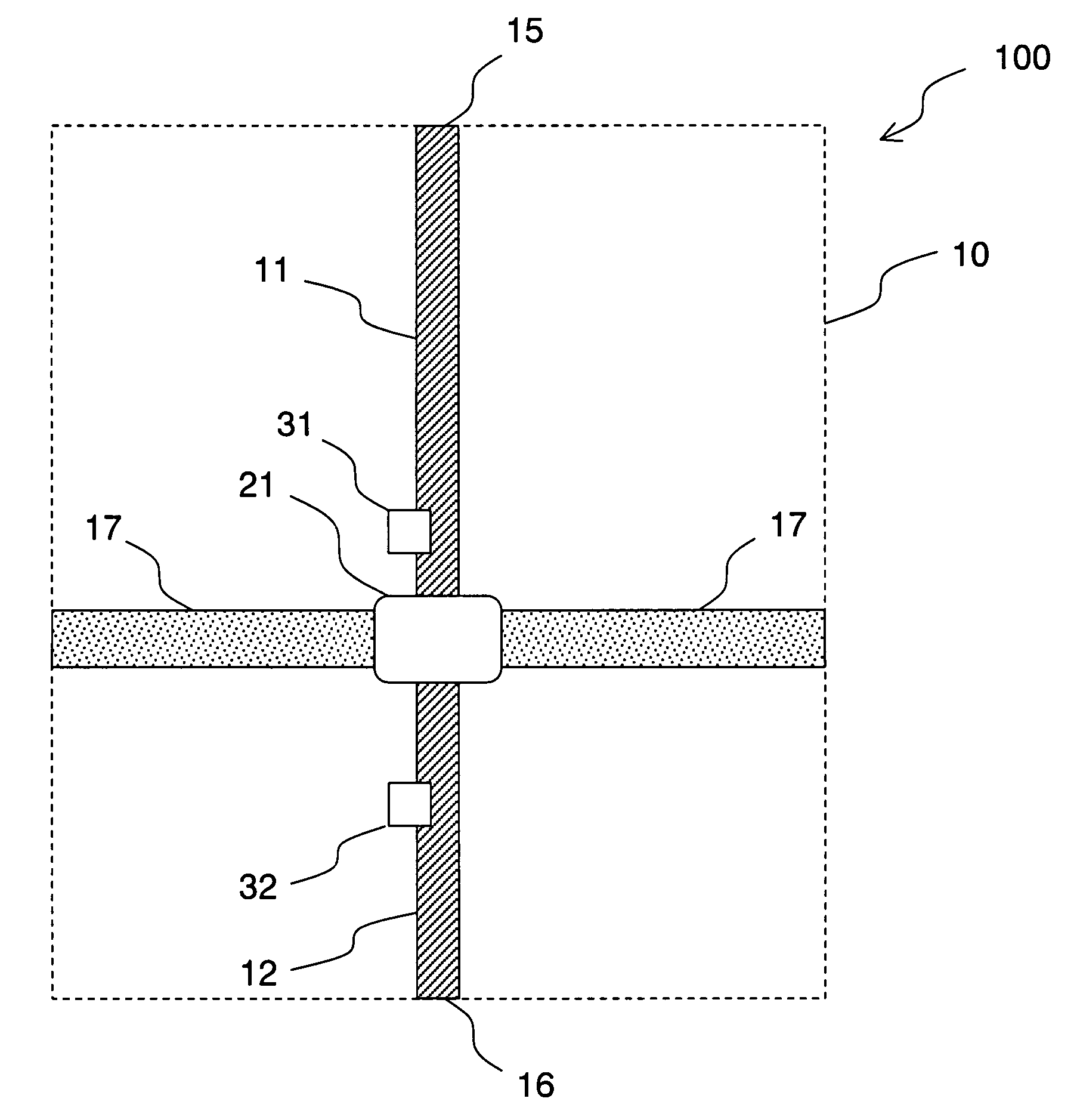
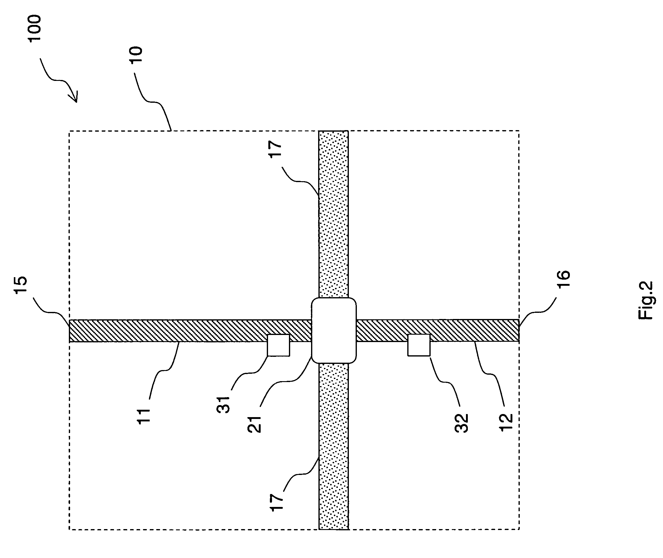
[0029]FIG. 2 is a structure drawing for explaining an example of the embodiment of the distributed constant circuit of the present invention. Referring to FIG. 2, reference numeral 10 denotes a substrate, reference numerals 11, 12 denote a micro strip line provided on the top face of the substrate 10, reference numeral 15 denotes an input terminal to the micro strip line 11, reference numeral 16 denotes an output terminal from the micro strip line 12, reference numeral 17 denotes a ground, reference numeral 21 denotes a semiconductor device as an electronic device, reference numerals 31, 32 denote a flat adjustment tab composed of conductor and reference numeral 100 denotes a distributed constant circuit.

[0030] The micro strip line is constituted of a ground formed on a s...


PUM


Abstract

According to a conventional art, a large number of adjustment pads are necessary if impedance mismatching is large or characteristic impedance is low. Such a large number of the adjustment pads needs to secure a large area for arrangement of the adjustment pads preliminarily. However, occupation of a large area induces an interference with other distributed constant circuit. The present invention concerns a distributed constant circuit capable of adjusting the impedance matching between a conductor line such as micro strip line disposed in a small area and an electronic device in order to solve the above-described problems. This distributed constant circuit intends to achieve the impedance matching between the characteristic impedance of the conductor line and the load impedance or drive impedance of the electronic device by bringing the adjustment tab moving on a substrate into a contact with the conductor line.

Description

BACKGROUND OF THE INVENTION [0001] 1. Field of the Invention [0002] The present invention relates to a distributed constant circuit capable of achieving impedance matching between a conductor line provided on the top face of a substrate and an electronic device connected to an input terminal or an output terminal and a method of adjusting the impedance matching of the distributed constant circuit. [0003] 2. Description of the Related Art [0004] When a conductor line or an electronic device connected to the conductor line is constituted on a substrate, sometimes impedance matching cannot be achieved between the characteristic impedance of the conductor line and load impedance or drive impedance of an electronic device. As causes for impedance mismatching, dispersion of dielectric constant or loss angle of substrate material, dielectric constant of conductive material of conductor line or length in minor axis thereof, dispersion of thickness of the conductor line, dispersion of impeda...

Claims


Application Information

Patent Timeline
IPC IPC(8): H03H7/38
CPCH01P3/081
Inventor IKEDA, HIROSHI
Owner TDK CORPARATION
Learn More