Optical head device, diffraction element and manufacturing method for diffraction element

Inactive Publication Date: 2005-01-06
NIDEC SANKYO CORP
View PDF4 Cites 23 Cited by
  • Summary
  • Abstract
  • Description
  • Claims
  • Application Information

AI Technical Summary

Benefits of technology

Also, in a conventional diffraction grating, the demultiplexing ratio of the zero-order light and the first-order diffracted lights is adjusted only from the step height and the duty ratio of the diffraction grating. However, in the diffraction element according to the present invention, the demultiplexing ratio of the zero-order light and the first order diffracted lights is capable of being easily adjusted by adjusting the areas of the first diffraction grating formed area and the second diffraction grating formed area. Therefore, the degree of freedom of a design is remarkably widened and thus the optimal diffraction element with a high degree of efficiency is obtained with respect to the first and the second laser beams. In addition, the diffraction element according to the present invention can be applied to a twin laser in which the first and the second laser light sources are mounted within one package.
Moreover, according to the present invention, the diffraction element can be disposed on the common optical path and thus capable of being positioned away from the first and the second laser light sources. Therefore, the pitch of the diffraction grating in the first and the second diffraction gratings can be widened. Accordingly, the first and the second diffraction gratings can be easily formed in mass production. Further, according to the diffraction element in which the first and the second diffraction gratings are formed on the same side face of the diffraction element, the diffraction element is suitable for mass production even by using a molding die or by semiconductor process in comparison with the conventional diffraction element in which the first and the second diffraction gratings are formed on the entire surface of both sides of the diffraction element.
In other words, when the diffraction element is produced by a molding die, the first and the second d

Problems solved by technology

Accordingly, when the diffraction grating is formed by semiconductor process such as film forming technique and photo lithography technique, an expensive exposure equipment such as a stepper is required.
Therefore, both the methods are

Method used


Image

  • Optical head device, diffraction element and manufacturing method for diffraction element
  • Optical head device, diffraction element and manufacturing method for diffraction element
  • Optical head device, diffraction element and manufacturing method for diffraction element

Examples


Example

Embodiment 1

Overall Construction

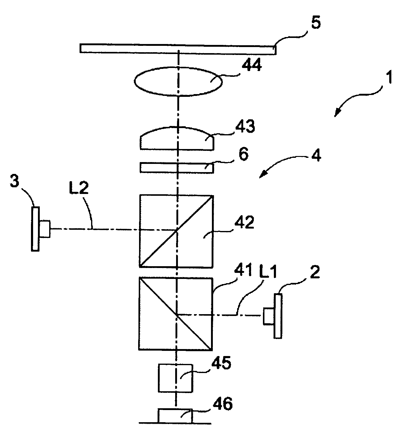
FIG. 1 is a schematic constructional view which shows an optical system of an optical head device in accordance with a first embodiment of the present invention. The optical head device 1 in the first embodiment of the present invention is capable of reproducing and / or recording information to a plural types of optical recording media 5 such as a DVD-R and a CD-R, which are different in the substrate thickness and recording density. The optical head device 1 includes a first laser diode 2 emitting a first laser beam L1 with a wavelength of 650 nm band, a second laser diode 3 emitting a second laser beam L2 with a wavelength of 780 nm band, and a common optical system 4.

The common optical system 4 includes a first beam splitter 41 which reflects the first laser beam L1 to an optical recording medium 5, a second beam splitter 42 which transmits the first laser beam L1 reflected by the first beam splitter 41 and reflects the second laser beam L2 to...

Example

FIG. 2(A) is a plan view of the diffraction element in accordance with the first embodiment of the present invention, FIG. 2(B) is its right side view, and FIG. 2(C) is a transverse cross-sectional view schematically showing the diffraction grating of the diffraction element shown in FIG. 2(A). FIG. 2(D) is an explanatory view showing diffracting state of the first laser beam L1 by the diffraction element 6 and FIG. 2(E) is an explanatory view showing diffracting state of the second laser beam L2 by the diffraction element 6.

As shown in these drawings, the diffraction element 6 is formed of a rectangular translucent substrate 61 which is made of a translucent material. The translucent substrate 61 is provided with an incident face 62 for the first laser beam L1 and the second laser beam L2 on one side and an emitting face 63 on the other side. The beam diameter of the first laser beam L1 is shown in FIG. 2(D) and the beam diameter of the second laser beam L2 is shown in FIG. 2(E)....

Example

Embodiment 2

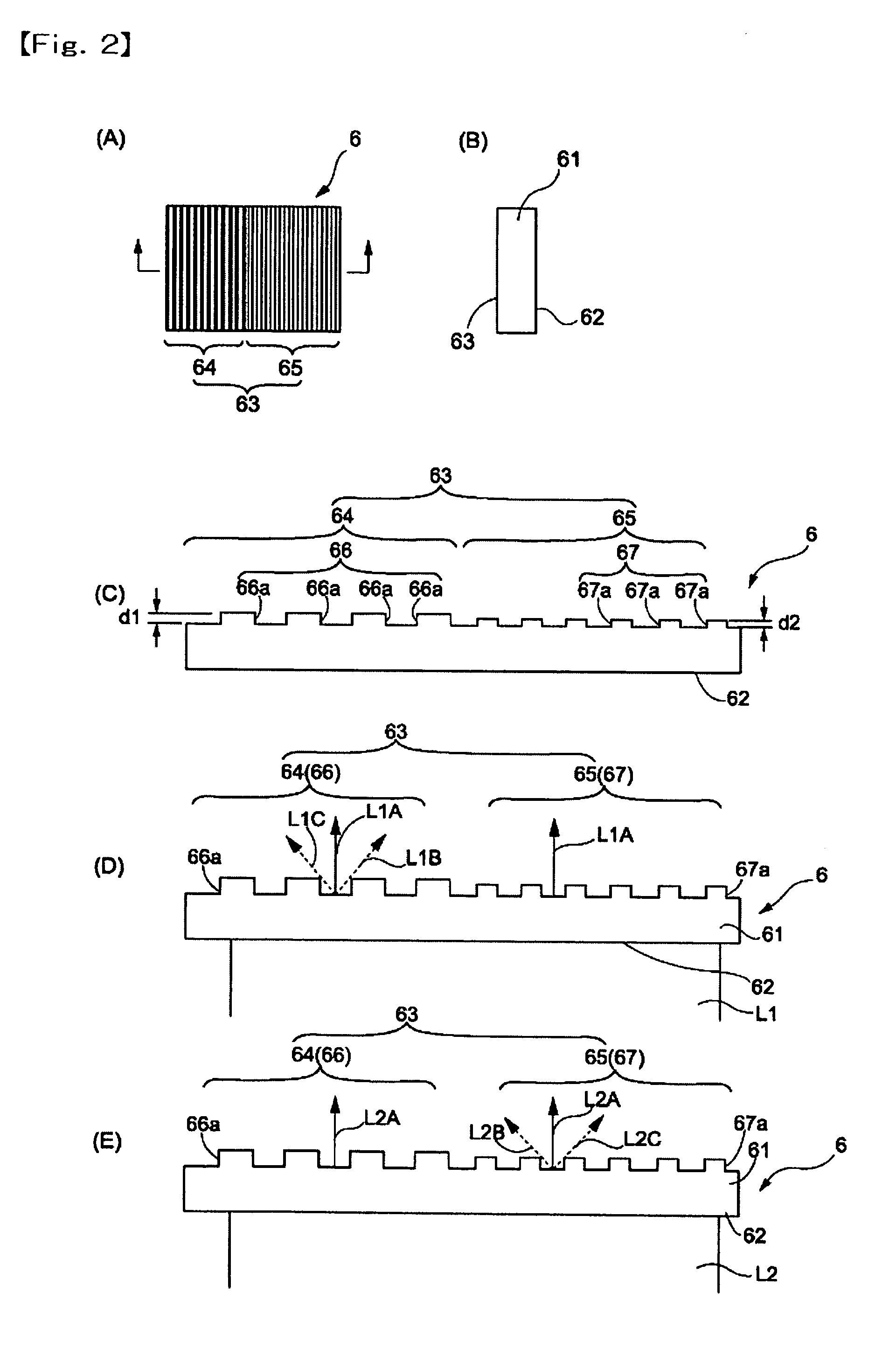
The diffraction element 6 in the first embodiment is constituted such that the emitting face 63 is divided into two areas of the first diffraction grating formed area 64 and the second diffraction grating formed area 65. However, the emitting face 63 may be divided into a plurality of areas in a stripe shape in which the first diffraction grating formed area 64 and the second diffraction grating formed area 65 are alternately disposed. In this case, the generation of the diffracted lights due to dividing the emitting face 63 into plural areas can be suppressed, for example, by setting the width of one stripe to be about 100 times of the wavelength to perform a satisfactory recording and reproduction.


PUM


Abstract

An optical head device includes a first light source which emits a first laser beam, a second light source which emits a second laser beam, a common optical path for guiding the first laser beam or the second laser beam to an optical recording medium, and a diffraction element disposed on the common optical path. The diffraction element includes a partially formed first diffraction grating such that the first laser beam is diffracted and the second laser beam is transmitted without being diffracted and a partially formed second diffraction grating such that the second laser beam is diffracted and the first laser beam is transmitted. The partially formed first diffraction grating and the partially formed second diffraction grating are formed in a side by side relation.

Description

CROSS-REFERENCE TO RELATED APPLICATIONS This application claims priority to Japanese Application No. 2003-108204 filed Apr. 11, 2003 and priority to Japanese Application No. 2003-394179 filed Nov. 25, 2003, which are incorporated herein by reference. BACKGROUND OF THE INVENTION 1. Field of the Invention The present invention relates to an optical head device which is used for reproducing from and / or recording to an optical recording medium such as a DVD or a CD, and a diffraction element for the optical head device and a manufacturing method for the diffraction element. 2. Description of the Related Art A two-wavelength optical head device has been known as an optical head device, which is provided with a laser diode for emitting a laser beam with a wavelength of 650 nm band for reproducing from and recording in a DVD-R and a laser diode for emitting a laser beam with a wavelength of 780 nm band for reproducing from and recording in a CD-R. For example, as shown in FIG. 9, a t...

Claims


Application Information

Patent Timeline
IPC IPC(8): G11B7/00G11B7/125G02B5/18G11B7/1275G11B7/135G11B7/1353G11B7/22
CPCG11B7/1275G11B2007/0006G11B7/22G11B7/1353
Inventor HAYASHI, KENICHI
Owner NIDEC SANKYO CORP
Why Eureka
Try Eureka