Drive circuit for electroluminescent device

a technology of drive circuit and electroluminescent device, which is applied in the direction of static indicating devices, instruments, etc., can solve the problems of difficult homogenization of the characteristics of tfts, deterioration of the quality of display such as non-uniform display production, and inability to perform uniform display. the effect of dispersing the characteristics of the drive transistor

Active Publication Date: 2006-10-05
GLOBAL OLED TECH
View PDF5 Cites 73 Cited by
  • Summary
  • Abstract
  • Description
  • Claims
  • Application Information

AI Technical Summary

Benefits of technology

[0018] As described above, according to the present invention, a voltage according to a threshold voltage of a drive transistor is set to the gate of the drive transistor by a constant current from a c

Problems solved by technology

Consequently, if dispersion of the characteristics of the drive transistors T1 occurs, the display of a uniform gradation cannot be performed, and the deterioration of the qual

Method used


Image

  • Drive circuit for electroluminescent device
  • Drive circuit for electroluminescent device
  • Drive circuit for electroluminescent device

Examples


example 1

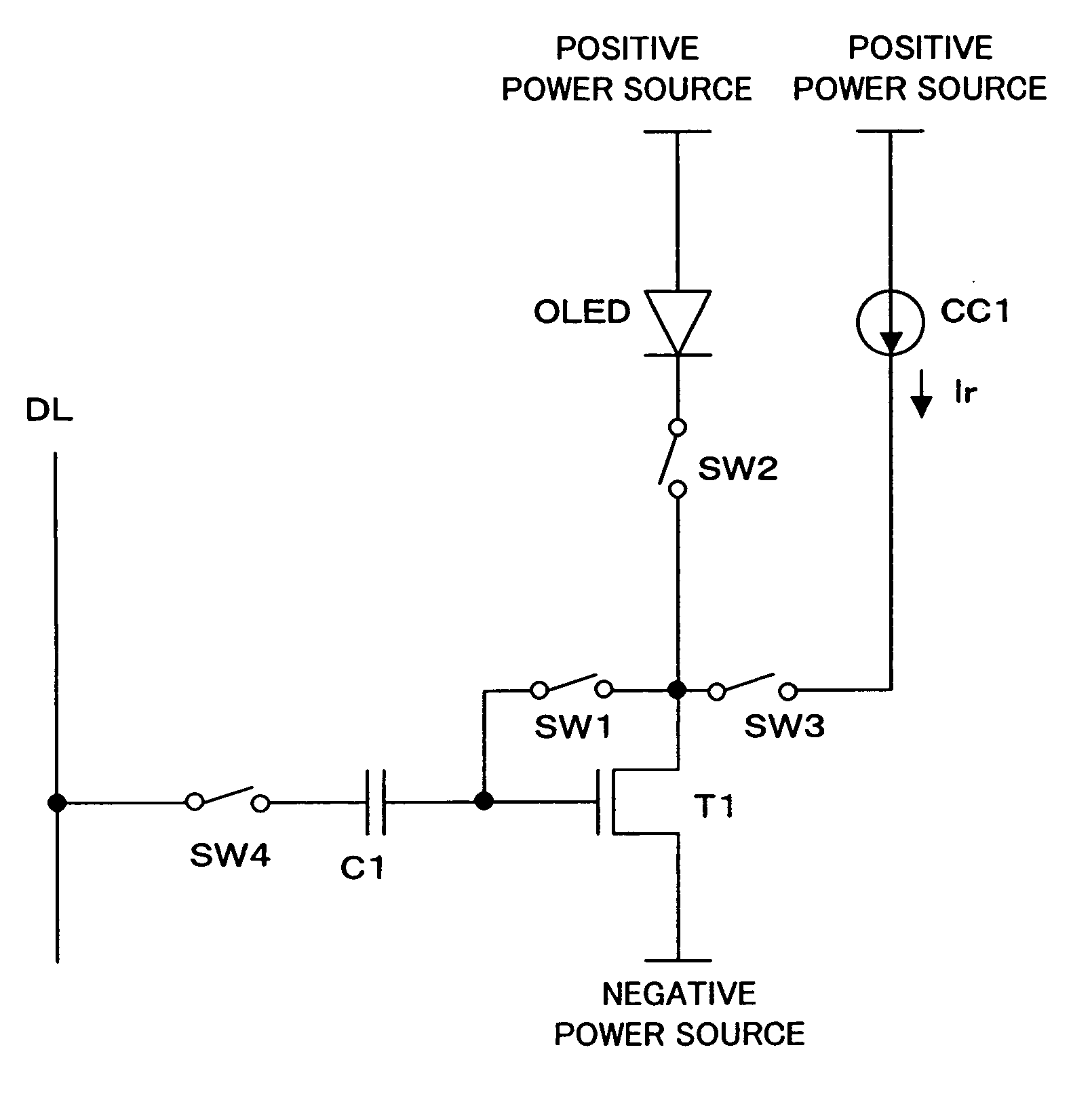
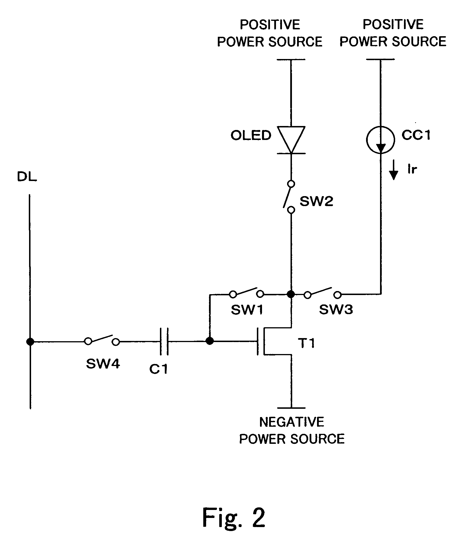
[0045] An example of a circuit realizing the driving of the present invention is shown in FIG. 3. As in the configuration shown in FIG. 2, switches SW1, SW2, and SW3 are arranged between the drain of the drive transistor T1 and the gate thereof; between the drain of the drive transistor T1 and the cathode of the organic EL device OLED; and between the drain of the drive transistor T1 and the constant current source CC1, respectively. Moreover, the switch SW4 is provided between the capacitor C1 and the signal line DL. Furthermore, in the example of FIG. 3, the connecting point of the switch SW4 and the capacitor C1 is connected to the negative power source through a switch SW5.

[0046] Moreover, all of the switches SW1-SW5 are composed of n-channel TFTs. The gates of the switches SW1, SW3, and SW4 are connected to a control line 1; the gate of the switch SW2 is connected to a control line 2; and the gate of the switch SW5 is connected to a control line 3.

[0047] In this circuit, the ...


PUM


Abstract

A drive circuit that compensates for the dispersion of the characteristics of drive transistors is disclosed. A switch SW2 is turned off, and switches SW1 and SW3 are turned on. Thereby, a constant current from a constant current source CC1 is flown in a drive transistor T1. Consequently, a gate voltage corresponding to the constant current Is written in the gate of the drive transistor T1. Then, the switches SW1 and SW3 are turned off, and the switch SW2 is turned on. Simultaneously, the voltage of a capacitor C1 on the side of the switch SW4 is varied according to a signal voltage, and thereby the voltage is added to the gate of the drive transistor T1 to flow a current corresponding to the signal voltage in the drive transistor T1.

Description

FIELD OF THE INVENTION [0001] The present invention relates to a drive circuit of a current drive type light emitting device such as an organic electroluminescence (EL) device. BACKGROUND OF THE INVENTION [0002] Drive circuits using two thin film transistors (TFTs), such as the circuit shown in FIG. 1 can be used to drive an organic EL device (OLED). The circuit of FIG. 1 is composed of an n-channel writing transistor T2, a holding capacitor C and an n-channel drive transistor T1. The drain of the writing transistor T2 is connected to a signal line DL, through which a signal voltage is supplied; the source thereof is connected to the gate of the drive transistor T1 and one end of the holding capacitor C; and the gate thereof is connected to a control line, through which a selection signal is supplied. Consequently, the signal voltage on the signal line DL is supplied to the one end (the gate of the transistor T1) of the holding capacitor C by raising the control line to an H level. ...

Claims


Application Information

Patent Timeline
IPC IPC(8): G09G3/30
CPCG09G3/325G09G2300/043G09G2310/0262G09G2300/0866G09G2310/0251G09G2300/0842
Inventor MIWA, KOICHI
Owner GLOBAL OLED TECH
Why Eureka
Try Eureka