Electrooptic device, substrate therefor, method for making the electrooptic device, and electronic apparatus

a technology of electrooptic devices and substrates, applied in the direction of semiconductor devices, optics, instruments, etc., can solve the problems of degrading contact properties, non-uniform resistance, and increasing the cost of electrooptic device production, so as to improve the contact properties of electrical connections, prevent separation and cracking, and high-quality image display

Active Publication Date: 2007-03-15
SEIKO EPSON CORP
View PDF3 Cites 57 Cited by
  • Summary
  • Abstract
  • Description
  • Claims
  • Application Information

AI Technical Summary

Benefits of technology

[0015] An advantage of the invention is that it provides an electrooptic device that can provide high-quality image display by improving the contact properties related to the electrical connection between the pixel electrode and the conductive layer while preventing the separation and cracking of the pixel electrode and the like, a substrate for the electrooptic device, a method for making the electrooptic device, and various types of electronic apparatuses having the electrooptic device.
[0016] A first aspect of the invention provides an electrooptic device including a substrate and a plurality of pixel units. Each pixel unit includes a pixel electrode; an active element for active control of the pixel electrode; a conductive layer that is formed below the pixel electrode and that connects the active element to the pixel electrode; an organic resin film that provides interlayer insulation between the active element and the pixel electrode and between the conductive layer and the pixel electrode, the organic resin film having a small hole that overlaps part of the conductive layer in a plan view; a first inorganic insulating film disposed between the organic resin film and the conductive layer and between the organic resin film and the active element such that the first inorganic insulating film overlaps the conductive layer and the active element in a plan view, the first inorganic insulating film having a first hole inside the small hole in a plan view, the first hole having a diameter equal to or smaller than the bottom of the small hole; and a second inorganic insulating film disposed between the organic resin film and the pixel electrode, the second inorganic insulating film having a second hole that is continuous to the first hole and that forms a contact hole together with the first hole. The pixel electrode is formed in a continuous manner from inside the contact hole to outside the contact hole such that the pixel electrode is electrically connected to the conductive layer exposed inside the first hole.
[0017] In this electrooptic device, for example, the pixel units are aligned in a predetermined pattern in an image display region on the substrate. During the operation by, for example, active matrix driving, the switching control and ON / OFF control of the pixel electrode composed of, for example, a transparent conductive film, is done by the active element. Alternatively, the active element may control the current supplied to the pixel electrode or the voltage applied to the pixel electrode. In each pixel unit, the active element is electrically connected to the pixel electrode through the conductive layer. For example, the drain of a TFT, which is an example of the active element, is connected to the pixel electrode through the conductive layer. Note that the substrate may be composed of a transparent material such as quartz, glass, or a semiconductor substrate, or a transparent sheet material such as plastic. The substrate is not limited to the transparent substrate and may be formed of a light-shielding material
[0018] The conductive layer is formed as a source or drain electrode of a TFT, which is an example of the active element, or may be disposed in the electrical path between the active element and the pixel electrode so as to function as a relay wire or relay electrode for relaying electrical connection between the active element and the pixel electrode.
[0019] In this electrooptic device, it is possible to form a multilayer-structure pixel unit in which active elements such as a pixel electrode and a pixel switching element, electrodes, and other associated components are formed in layers of different levels. Thus, for example, when compared with the structure of the pixel unit disclosed in J-P-A2003-308027, the aperture ratio can be increased. In this specification, the region in the pixel or pixel unit where light can be emitted from or where light can pass through is referred to as “opening region”. The area ratio of the opening region to the entire region of the pixel (i.e., the opening region and the non-opening region) is referred to as the “aperture ratio”.
[0020] The pixel electrode is isolated from the active element and the conductive layer disposed below the pixel electrode by an organic resin film composed of a photosensitive resin such as acryl. The first inorganic insulating film composed of a nitrogen-containing material is formed below the organic resin film and above the active element and the conductive layer. The first inorganic insulating film is provided as a protective film for preventing the water in the water-absorbent organic resin film from further dispersing into the active element and the conductive layer. The first inorganic insulating film is formed to overlap the active element and the conductive layer in a plan view. Thus, the surface of the conductive layer is substantially completely covered with the first inorganic insulating film except in part where electrical connection to the pixel electrode is needed. Thus, the conductive layer does not generally come into direct contact with the organic resin film. The first inorganic insulating film is preferably formed as a base of the organic resin film so that the first inorganic insulting film can prevent water below from entering the organic resin film.

Problems solved by technology

Thus, after forming the small hole, an organic substance derived from the organic resin film may remain on the surface of the conductive layer, and this increases the resistance related to the electrical connection between the pixel electrode and the conductive layer, i.e., the contact resistance, and makes the contact resistance non-uniform among contact holes, thereby disadvantageously degrading the contact properties.
In order to overcome this problem, cumbersome procedures such as modifying design of wiring that constitutes the pixel unit are necessary, and the cost required for the production of the electrooptic device may thus increase.

Method used


Image

  • Electrooptic device, substrate therefor, method for making the electrooptic device, and electronic apparatus
  • Electrooptic device, substrate therefor, method for making the electrooptic device, and electronic apparatus
  • Electrooptic device, substrate therefor, method for making the electrooptic device, and electronic apparatus

Examples


first embodiment

[0076] A first embodiment of the present invention will now be described with reference to FIGS. 1 to 11. In this embodiment, the invention is applied to an active matrix transmissive liquid crystal device.

1.1 Overall Structure of Liquid Crystal Device

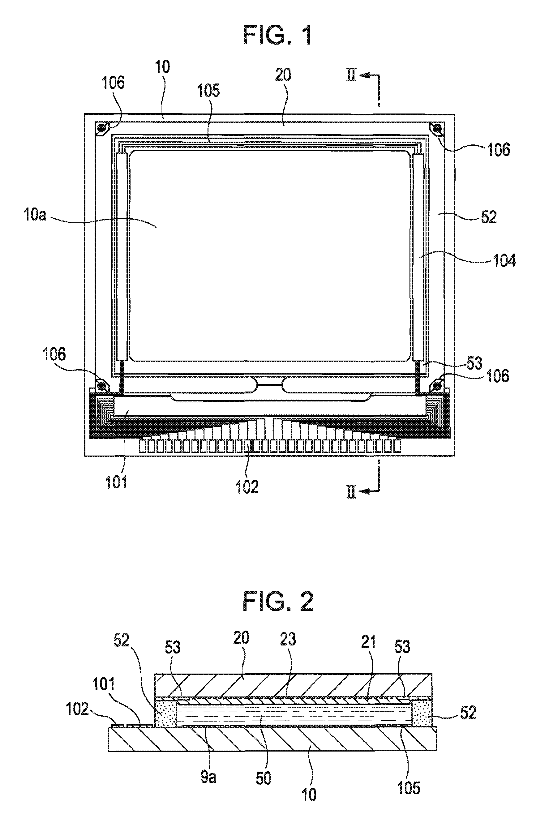
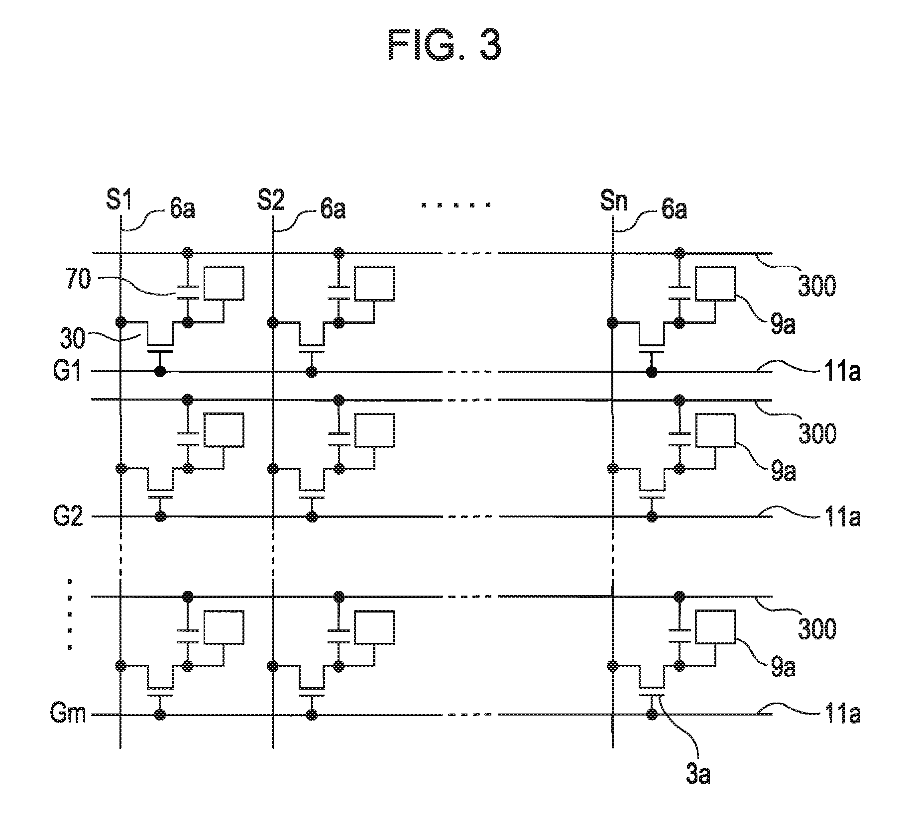
[0077] First, the overall structure of the liquid crystal device of this embodiment will be described with reference to FIGS. 1 to 3. FIG. 1 is a plan view of a liquid crystal device viewed from the counter substrate-side. FIG. 2 is a cross-sectional view taken along line II-II in FIG. 1.

[0078] As shown in FIG. 2, in this liquid crystal device, a TFT array substrate 10, which is an example of the substrate according to the present invention, and a counter substrate 20 are arranged opposite each other and a liquid crystal layer 50 is sealed between the TFT array substrate 10 and the counter substrate 20.

[0079] The TFT array substrate 10 and the counter substrate 20 are bonded to each other with a sealing member 52 disposed in a sea...

second embodiment

2. Second Embodiment

[0128] A second embodiment of the electrooptic device will now be described with reference to FIGS. 12 and 13. The second embodiment differs from the first embodiment in that it has a reflector film. Thus, only the differences from the first embodiment are described with reference to FIGS. 12 and 13. For alike components, some may be described with reference to FIGS. 1 to 7B while descriptions for others are omitted to avoid redundancy. In the description below, the electrooptic device is applied to a reflective liquid crystal device.

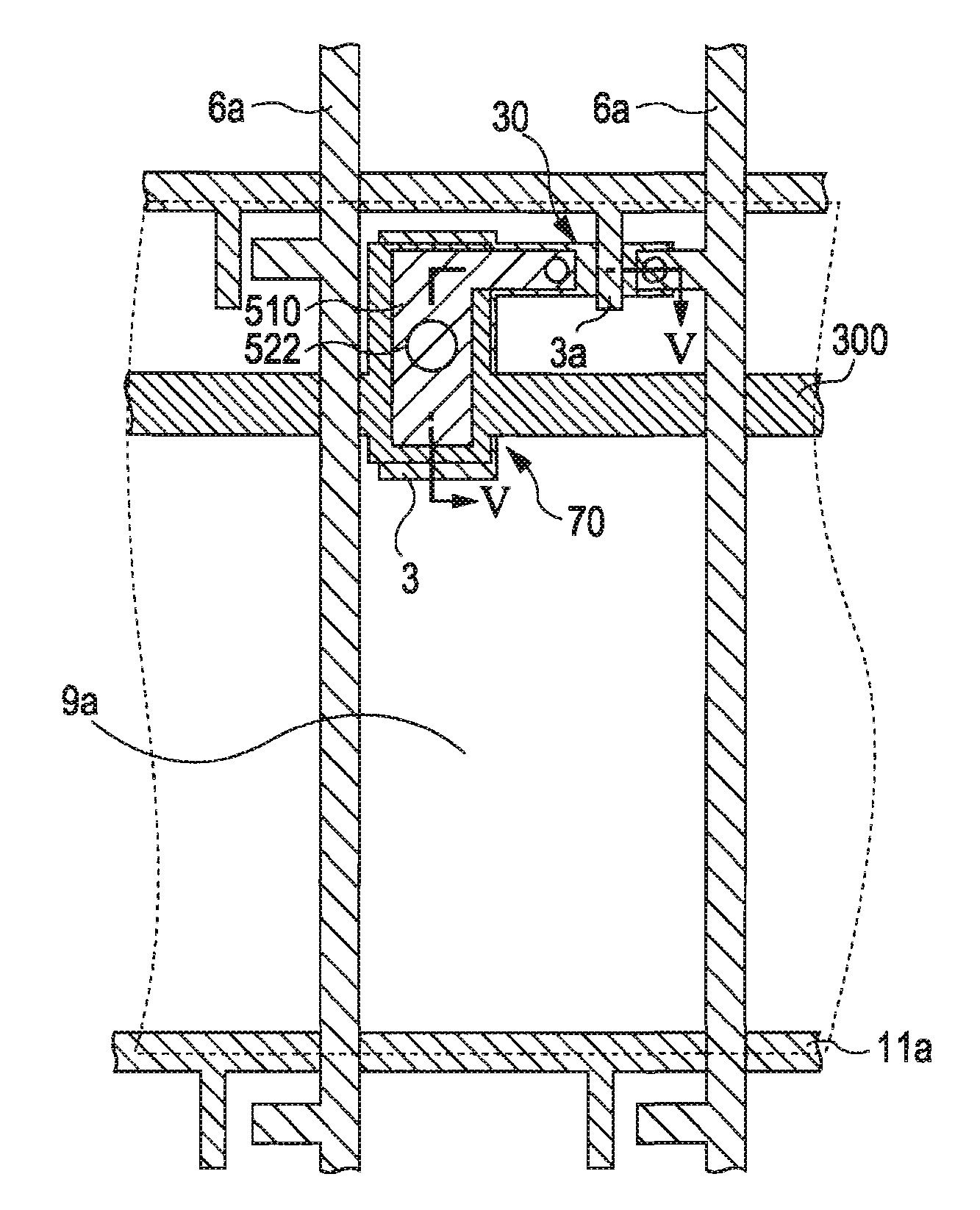
[0129]FIG. 12 is a cross-sectional view equivalent to the cross-sectional view of FIG. 5, showing an arbitrarily selected pixel unit.

[0130] Referring to FIG. 12, a reflector film 85 composed of silver or an aluminum (Al)-containing material is formed on the organic resin film 80 and outside the small hole 520. When each pixel unit is viewed in a plan view from above the TFT array substrate 10, the reflector film 85 of each pixel un...

third embodiment

3. Third Embodiment

[0140] A third embodiment of the electrooptic device will now be described with reference to FIGS. 14 to 17. The electrooptic device of the third embodiment is an organic EL device of an active matrix type. In the description below, the structures common to the first and second embodiments are referred to as the same reference numerals in FIGS. 1 to 13B and described with reference to these drawings. However, some descriptions are omitted to avoid redundancy.

3.1 Overall Structure of Organic EL Device

[0141] The overall structure of the organic EL device will first be described with reference to FIG. 14. FIG. 14 is a block diagram showing the overall structure of the organic EL, device of the third embodiment.

[0142] In the image display region 110 of the organic EL device, the data lines 114 and the scan lines 112 running across each other are provided. Pixel units 700 correspond to the intersections of these lines and are arranged in a matrix. In the image disp...


PUM

PropertyMeasurementUnit
contact resistanceaaaaaaaaaa
conductiveaaaaaaaaaa

Abstract

An electrooptic device includes a substrate and a pluralty of pixel units. Each pixel unit includes a pixel electrode; an active element for active control of the pixel electrode; a conductive layer that is disposed below the pixel electrode and that connects the active element to the pixel electrode; an organic resin film that provides interlayer insulation between the active element and the pixel electrode and between the conductive layer and the pixel electrode, the organic resin film having a small hole that overlaps part of the conductive layer in a plan view; a first inorganic insulating film disposed between the organic resin film and the conductive layer and between the organic resin film and the active element such that the first inorganic insulating film overlaps the conductive layer and the active element in a plan view, the first inorganic insulating film having a first hole inside the small hole in a plan view, the first hole having a diameter equal to or smaller than the bottom of the small hole; and a second inorganic insulating film disposed between the organic resin film and the pixel electrode, the second inorganic insulating film having a second hole that is continuous to the first hole and that forms a contact hole together with the first hole. The pixel electrode is formed in a continuous manner from inside the contact hole to outside the contact hole such that the pixel electrode is electrically connected to the conductive layer exposed inside the first hole.

Description

[0001] The entire disclosure of Japanese Application Nos. 2005-261715, filed Sep. 9, 2005 and 2006-187522, filed Jul. 7, 2006 are expressly incorporated by reference herein. BACKGROUND [0002] 1. Technical Field [0003] The present invention relates to the technical field pertaining to substrates for electrooptic devices such as organic electro-luminescence (EL) devices or liquid crystal devices, electrooptic devices including such substrates, methods for making the electrooptic devices, and electronic apparatuses including the electrooptic devices. [0004] 2. Related Art [0005] Electrooptic devices of this type display images by controlling switching of pixel electrodes by using pixel switching elements in the individual pixel sections through an active matrix driving technology, for example. [0006] On a substrate, a pixel electrode is formed in a layer different from that of a pixel switching element, and a conductive layer, a relay layer, or a relay electrode is formed to provide el...

Claims


Application Information

Patent Timeline
Patent Type & Authority Applications(United States)
IPC IPC(8): G02F1/136
CPCG02F1/133345G02F1/136227H01L51/5271H01L27/3258H01L27/3248H10K59/123H10K59/124H10K50/856
Inventor EGUCHI, TSUKASA
Owner SEIKO EPSON CORP
Why Eureka
Try Eureka