However, it has been found out by the present inventors that there is a fear that when a probe is brought into direct contact with each bonding pad, the bonding pad is endamaged and a failure in connection to each
relocation wiring occurs.
As to the reference described in the
paragraph (d), however, there is a possibility that when a probe is applied to one of bonding pads antecedent to a relocation wiring process, the surface of the bonding pad will damage and the reliability of connection to a relocation wiring layer will be degraded, as discussed above by the present inventors.
A limitation is imposed on the selection of a relocation wiring material.
It has been revealed by the present inventors that the technology described in the
paragraph (e) also has the possibility that each under solder bump
metallurgy will be endamaged at a probe tip in a manner similar to the technology described in the
paragraph (d), and has led to degradation in wettability relative to solder and degradation in reliability of connections to each solder bump
electrode due to the damage of a barrier
metal used for the prevention of solder
diffusion.
Therefore, it has been revealed by the present inventors that each of the technologies described in the References (e) and (f) has a new problem in that it is difficult to apply a normally-used
cantilever type probe to under bump metallurgies or testing pads arranged in a multiple row, and terminal-dedicated expensive probes disposed in area array form are additionally required.
It has been found out by the present inventors that the Reference described in the paragraph (g) has a problem in that when the size of each bonding pad and the interval between the bonding pads become narrow with high integration of a
semiconductor device, the sizes of the testing pads and the interval therebetween become also narrow, and the positioning of each probe and reliable contact thereof fall into difficulties.
It has been revealed by the present inventors that each of the References described in the paragraphs (f) through (h) is accompanied by a problem that since the testing pads are formed on an inorganic insulating layer or a
metal wiring layer, the surface of each testing pad is hard to deform where a
hard metal film such as
chromium,
nickel or the like is used for the testing pads, and hence the contactability with a probe tip is poor, and an expensive probe whose tip is given
gold plating and which has adopted a structure capable of obtaining a wide contact area, is required.
Further, as described as the prior arts in the paragraphs (e) through (h), a problem has been revealed that when the probe is applied to the already-formed solder bump, the probe is applied to a curved surface covered with a thick
oxide film under a strong load, whereby the bump is apt to deform and the probe per se is easy to undergo damage.
Namely, the prior arts do not lead to the provision of the inventive concept that focused attention on the testing pads dedicated for testing, which are used only for probe testing or inspection and unnecessary at the final product stage.
Thus, the present inventors have revealed that if the solder bump electrodes are provided even for
signal terminals necessary only for testing, then the number of the bump electrodes increases and the
layout of the bump electrodes at practical intervals falls into difficulties from the meaning of mounting thereof to a circuit substrate.
The first problem is that the process of defining the window for applying the
laser light therethrough is becoming very difficult.
Thus, since the thickness of the insulating film from the polysilicon fuse to the top
passivation film reaches 5 μm or more, it is technically difficult to uniformly effect
etching for leaving the insulating film to a thickness of about 0.5 μm at a fuse upper portion on the whole surface of the
wafer.
When the thickness of the insulating film at the fuse upper portion is left 1 μm or more, the incident intensity of
laser light becomes weak and the melting-down or blowing of the fuse becomes insufficient.
When the thickness of the insulating film at the fuse upper portion is thinned to 0.5 μm or less, there is in danger of the surface of the fuse being exposed depending on variations in the subsequent process treatment.
The second problem is that the fuse cannot be blown by the conventional
radiation of
laser light from the viewpoint of the
system of the manufacturing process in the flip-
chip type semiconductor integrated circuit.
When the conventional
system for blowing the fuse through the
radiation of the
laser light is applied to the flip-chip type semiconductor integrated circuit, the deposition and
processing of each
metal wiring for constituting the relocation wring similar to the
lead frame at the upper portion of each blown fuse are performed, thereby resulting in unavoidance of degradation in reliability due to the
corrosion of the polysilicon fuse and entrance of
moisture from its corroded portion.
The third problem resides in that the polysilicon fuse needs a relatively large
layout area.
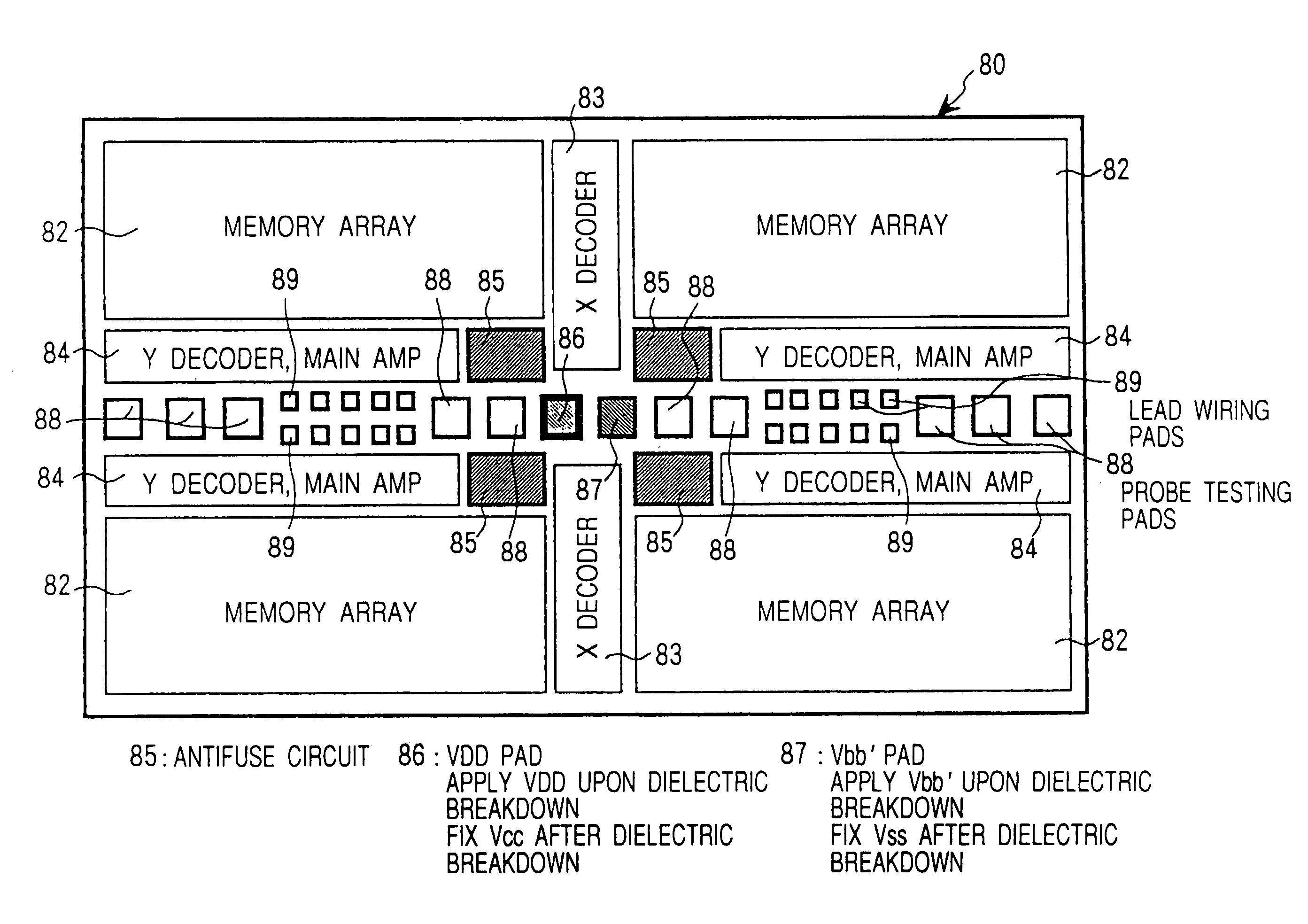
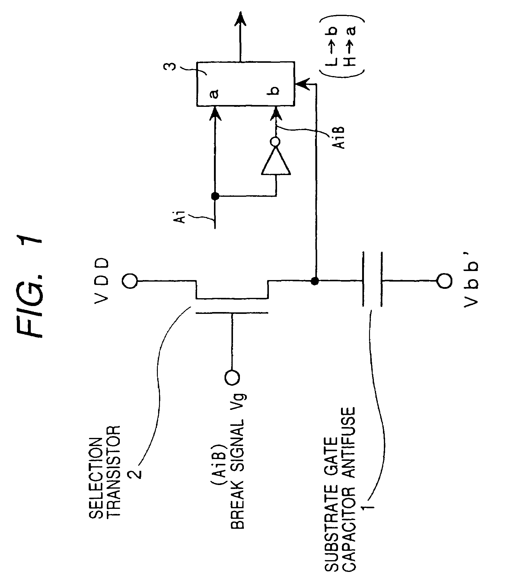
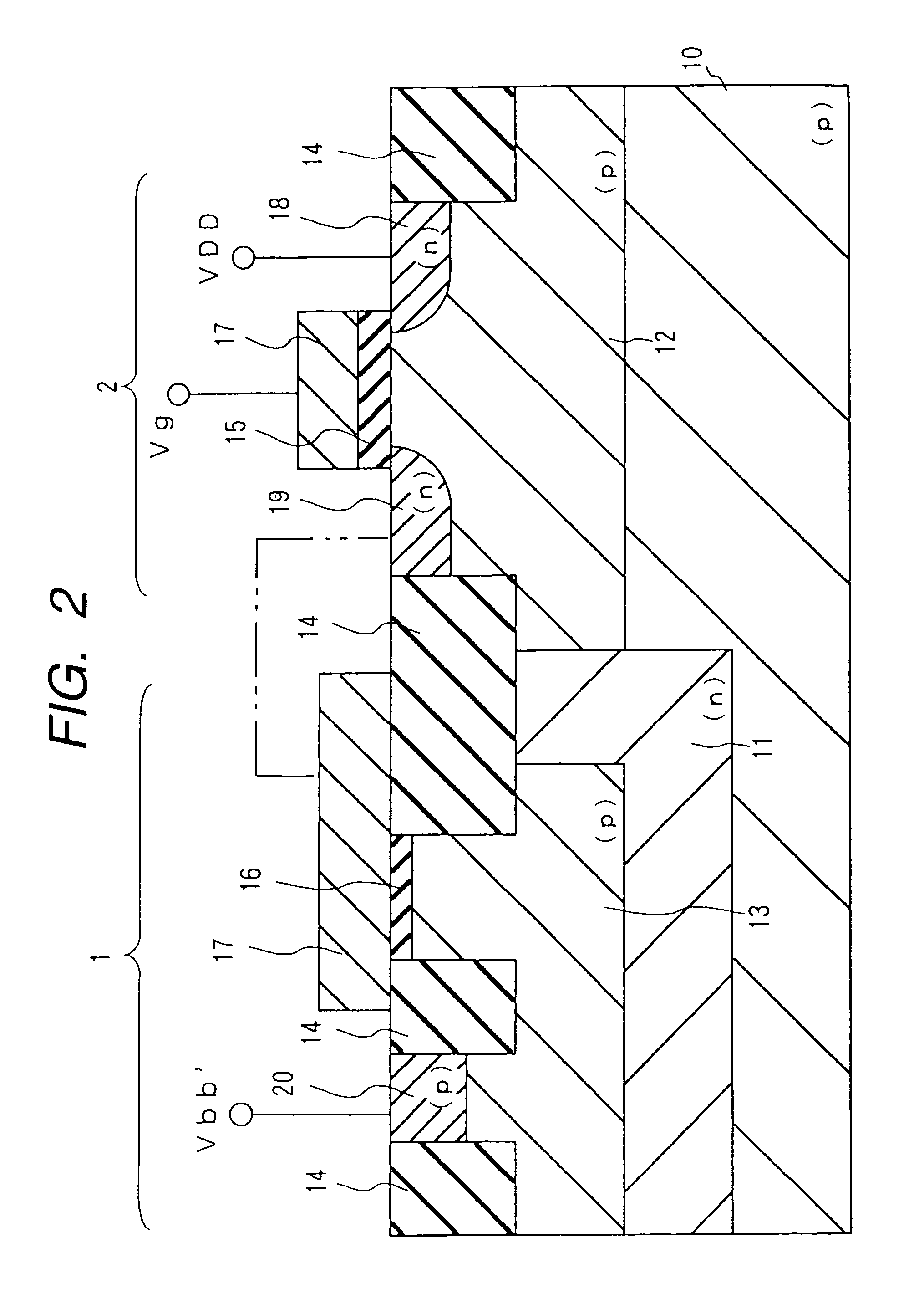
According to it, it has been revealed that when the number of the program elements may be low, a chip occupied area taken by
peripheral circuits used for electrical writing or the like relatively increases and hence area efficiency becomes disadvantageous.
Thus, the execution of the process like the bonding option is no longer physically impossible after
wafer processes are all completed.

