Optical wavelength division multiplexer

a wavelength division multiplexer and optical technology, applied in the field of optical wavelength division multiplexers, can solve the problems of increasing cost, increasing the problem of temperature variation, and excessive loss of about 2.0 db in principle, and achieve the effect of reducing excessive loss

Inactive Publication Date: 2006-10-05
NEC CORP
View PDF2 Cites 9 Cited by
  • Summary
  • Abstract
  • Description
  • Claims
  • Application Information

AI Technical Summary

Benefits of technology

[0023] An object of the invention is to provide an optical wavelength division multip

Problems solved by technology

However, in the system of controlling the chip temperature using a heater or the like to control the center wavelength, power supply is required and circuits for precise dynamic control are required to be incorporated and thereby, the requirements lead to cost increase.
Furthermore, since the wavelength of each device in each node must be controlled so as not to

Method used


Image

  • Optical wavelength division multiplexer
  • Optical wavelength division multiplexer
  • Optical wavelength division multiplexer

Examples


first embodiment

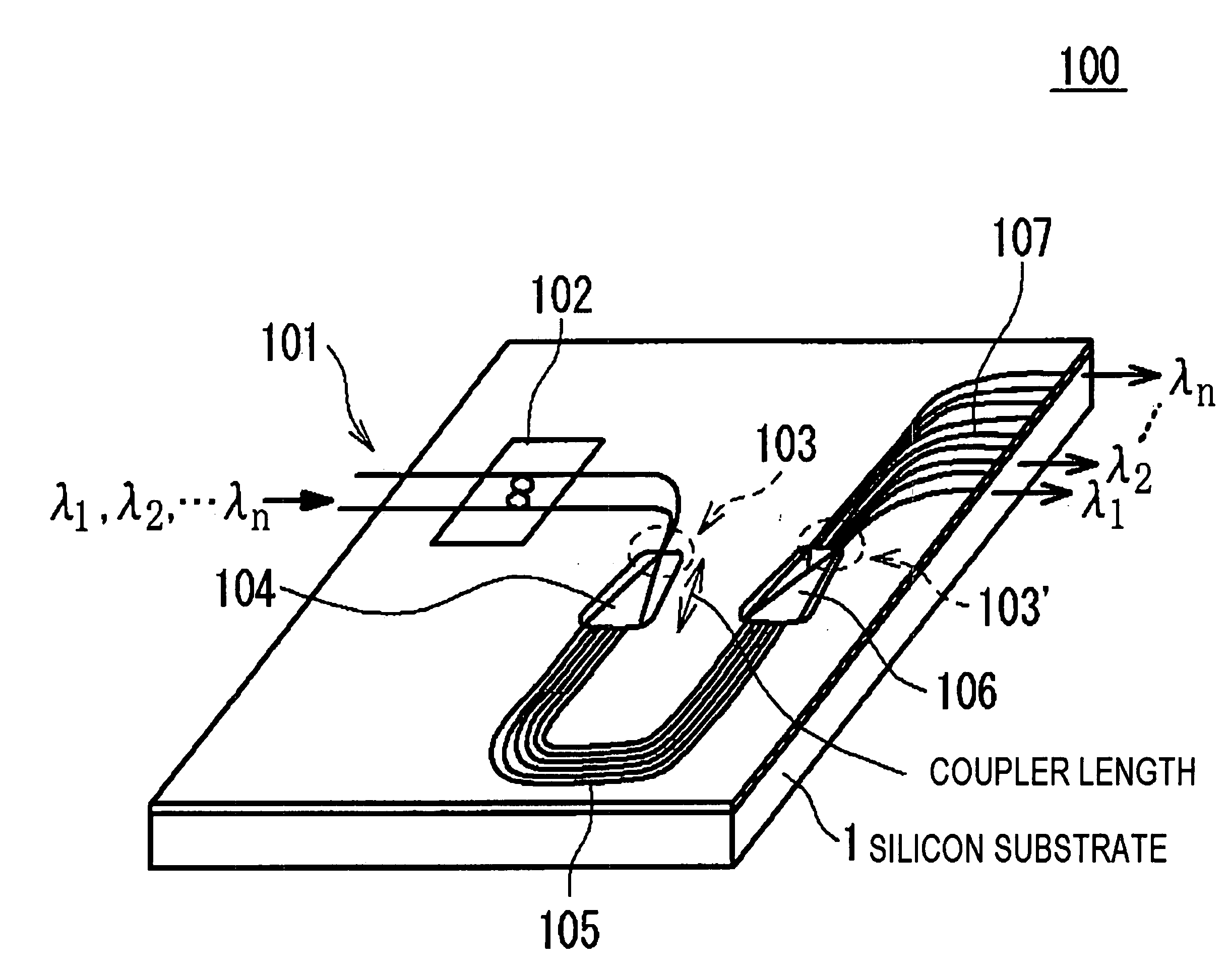
[0055] The first embodiment of the optical wavelength division multiplexer according to the invention will be described by referring to FIGS. 5, 6, and 8. FIG. 5 is a configuration diagram of the optical wavelength division multiplexer according to the invention. The optical wavelength division multiplexer according to the invention includes an arrayed waveguide grating 100, at least two input optical waveguides 101, and a flattening interferometer with ring resonator 102 containing a ring resonator. The flattening interferometer with ring resonator 102 is preferably cascade-connected to the arrayed waveguide grating 100. The arrayed waveguide grating 100 has a waveguide array 105 containing plural optical waveguides with different lengths and curvatures, an input side coupler optical waveguide 104 as a slab waveguide connected to the input side of the waveguide array 105, an output side coupler waveguide 106 as a slab waveguide connected to the output side of the waveguide array 10...

second embodiment

[0062] The second embodiment of the optical wavelength division multiplexer according to the invention will be described by referring to FIGS. 7, 14, and 15. The optical wavelength division multiplexer in the embodiment includes a flattening interferometer with ring resonator 102′ with Maximally flat filter structure in place of the flattening interferometer with ring resonator 102 in the first embodiment. As below, the same signs are attached to the same components as those in the first embodiment, and the description thereof will not be repeated.

[0063]FIG. 7 is a configuration diagram of the flattening interferometer with ring resonator 102′. Referring to FIG. 7, the flattening interferometer with ring resonator 102′ includes an input optical waveguide 301 connected to the input optical waveguides 101, output optical waveguides 304 and 305 connected to the coupler connecting part waveguide 103, a Mach-Zehnder interferometer 303, and a ring resonator 302. The ring resonator 302 is...

third embodiment

[0067] The third embodiment of the optical wavelength division multiplexer according to the invention will be described by referring to FIG. 16. The optical wavelength division multiplexer in the embodiment includes one output optical waveguide 304′ in place of the two output optical waveguides 304 and 305 connected to the Mach-Zehnder interferometer 303 in the second embodiment. In this regard, the output optical waveguide 304′ is connected to the Mach-Zehnder interferometer 303 via an optical directional coupler 308′. As below, the same signs are denoted to the same components as those in the first embodiment, and the description thereof will not be repeated.

[0068] The width of the optical waveguide in the embodiment has a width equal to or more than twice the optical waveguide width in the first and second embodiments, and the optical waveguide functions as a so-called multimode waveguide. The length of the interferometer in this case is expressed by the following equation.

L=(n...


PUM


Abstract

In an optical wavelength division multiplexer, flattening of band characteristic can be realized while reducing excessive loss due to the flattening of band characteristic in an arrayed waveguide grating. Further, the flat band of the band characteristic can be made broader.
The optical wavelength division multiplexer according to the invention includes: a first coupler optical waveguide 104 and a second coupler optical waveguide 106; one or more input side connecting part waveguide(s) 103 with one end connected to an input optical waveguide 101 and the other end connected to an optical input end face of the first coupler optical waveguide 104; one or more output side connecting part waveguide(s) 103′ with one end connected to an output optical waveguide 107 and the other end connected to an optical output end face of the second coupler optical waveguide 106; and an arrayed optical waveguide 105 connected between the first coupler optical waveguide 104 and the second coupler optical waveguide 106 and having plural channel waveguides with different lengths from one another, and further includes an optical interferometer connected to at least two optical waveguides between the input side connecting part waveguide 103 and the input optical waveguide 101. The optical interferometer includes a ring structure 202 that feeds back an input light, and is provided so that an interference period of the optical interferometer may become equal to a difference between frequencies of light output from adjacent optical waveguides of the output side connecting part waveguide 107.

Description

[0001] This application is based on Japanese Patent application NO. 2005-105253, the content of which is incorporated hereinto by reference. FIELD OF THE INVENTION [0002] The present invention relates to an optical wavelength division multiplexer, and specifically to an optical wavelength division multiplexer of an arrayed waveguide grating. RELATED ART [0003] With growing demand for communication, optical communication systems using DWDM (Dense Wavelength Division Multiplexing) are widely used in intercontinental and intercity large-capacity long-distance networks. The demand for waveguide type optical function devices such as AWG (Arrayed Waveguide Grating) devices as key components for the DWDM system is increasing. Since the arrayed waveguide grating can be fabricated in the same process and the same number of steps regardless of the number of channels and there is no characteristic degradation such as loss increase in principle, it is used as a key device for wavelength divisio...

Claims


Application Information

Patent Timeline
IPC IPC(8): G02B6/26
CPCG02B6/12007G02B6/12016G02B6/2938G02B6/29352G02B6/12019
Inventor SUZUKI, KOUICHIHINO, TOMOYUKI
Owner NEC CORP
Why Eureka
Try Eureka