

Solid-state image pickup device and the manufacture method thereof
- Summary
- Abstract
- Description
- Claims
- Application Information
AI Technical Summary
Benefits of technology
Problems solved by technology
Method used
Image

Examples
modified embodiment 1
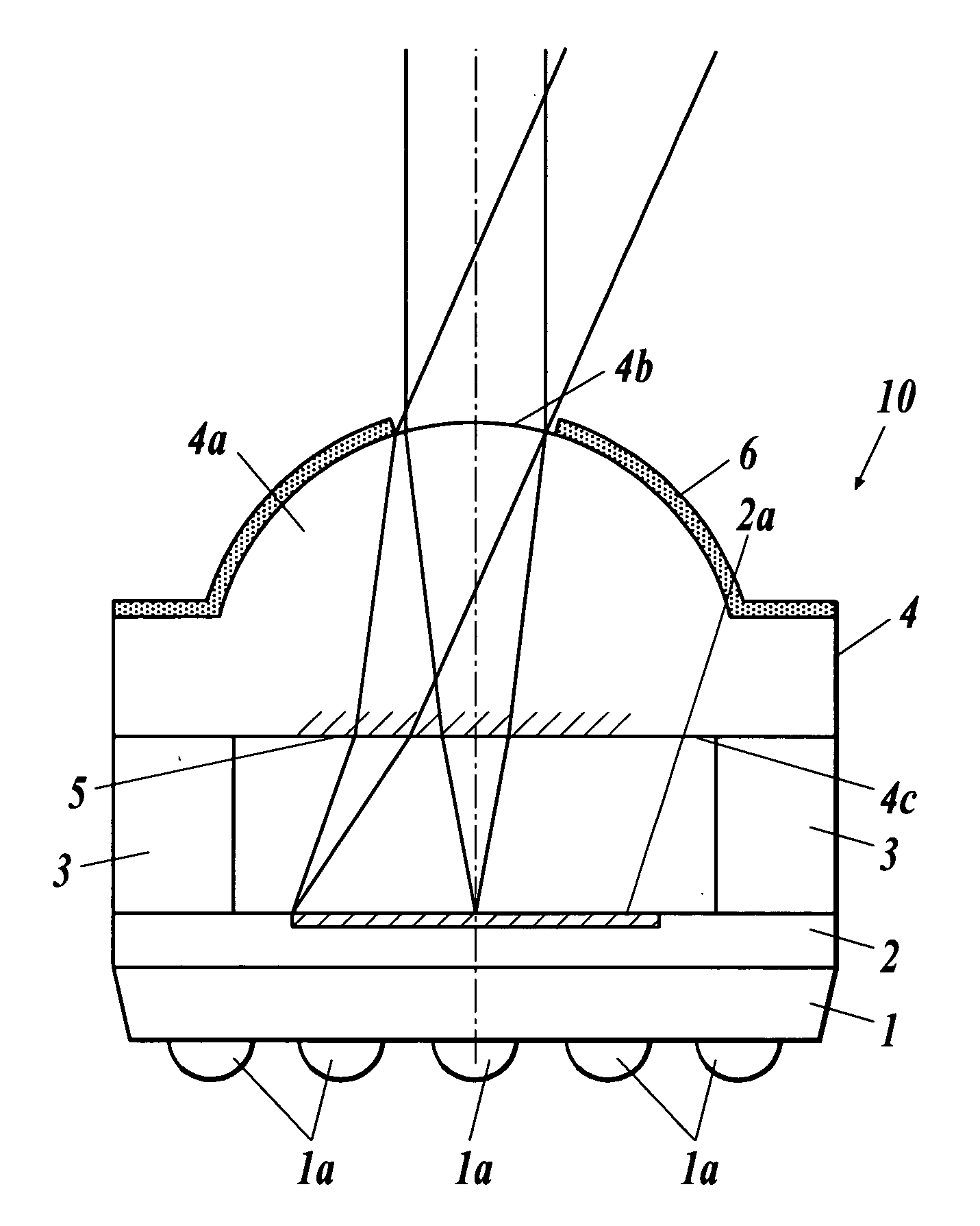
[0070]FIG. 4 illustrates a modified embodiment of the solid-state image pickup device 10 of FIG. 1 (solid-state image pickup device 20).
[0071] In the solid-state image pickup device 20 according to Modified Embodiment 1, a seal member 14 is composed of a plurality of components. Specifically, the seal member 14 is composed of a parallel flat plate 14A which is supported by the spacer member 3, an optical device 14B having an image pickup lens section 4a, and a doughnut plate-like aperture stop 16 which provided between the parallel flat plate 14A and the optical device 14B. The infrared ray cut filter coating 5 is formed on the image pickup lens side face 14c of the parallel flat plate 14A. The solid-state image pickup device 20 has the same structure as that of the embodiment of FIG. 1 except for the above. Thus, the same structure will not be further described by denoting the same components with the same reference numerals.
modified embodiment 2
[0072]FIG. 5 illustrates Modified Embodiment 2 of the solid-state image pickup device 10 of FIG. 1 (solid-state image pickup device 30).
[0073] As in the solid-state image pickup device 20 according to Modified Embodiment 1, the solid-state image pickup device 30 according to Modified Embodiment 2 also has the seal member 14 composed of a plurality of members. Specifically, the seal member 14 is composed of the parallel flat plate 14A, a second parallel flat plate 14C, and the aperture stop 16.
[0074] The solid-state image pickup device 20 according to Modified Embodiment 1 has the optical device 14B integrated with the image pickup lens section 4a. The solid-state image pickup device 30 according to Modified Embodiment 2 is different from the solid-state image pickup device 20 in that the second parallel flat plate 14C is separately provided from the solid image pickup lens section 4a. The solid-state image pickup device 30 has the same structure as those of the embodiments of FIG....
exemplary example 1
[0088] Exemplary Example 1 uses two glass substrates separated from one another as members corresponding to the parallel flat plate 14A and the second parallel flat plate 14C of FIG. 5. An image pickup lens section made of resin material is formed on a glass substrate. The respective glass substrates have therebetween an aperture stop. Data for this structure is shown below.
[0089] Tables 1 and 2 shown below show the data for this image pickup lens section. FIG. 6 to FIG. 8 show abberrations of the image pickup lens section.
TABLE 1f = 0.841 mm, F = 3.60, 2Y = 1.00 mm, fB = 0.450 mm(Object distance = 300 mm)Face No.R(mm)D(mm)Ndνd10.5490.181.6530022.32∞0.201.5163364.13∞0.02stop∞0.004∞0.201.5163364.15∞
[0090] In Table 1, “face No. 1” denotes an object side face of a part corresponding to the image pickup lens section 4a of FIG. 5, “face No. 2” denotes an image side face of this part, “face No. 3” denotes an image side face of a glass substrate corresponding to the second parallel flat...
PUM
 Abstract
Description
Claims
Application Information