Thin film resistor head structure and method for reducing head resistivity variance

a thin film resistor and resistor head technology, applied in resistor manufacturing, semiconductor devices, semiconductor/solid-state device details, etc., can solve the problems of insufficient removal of undesired metallization residues, and inability to meet the requirements of many conventional integrated circuit processing steps. , to achieve the effect of reducing or eliminating the inaccuracy of the resistance and the ratio of the resistance of the thin film resistor head,

Active Publication Date: 2006-10-12
TEXAS INSTR INC
View PDF3 Cites 17 Cited by
  • Summary
  • Abstract
  • Description
  • Claims
  • Application Information

AI Technical Summary

Benefits of technology

[0019] It is an object of the invention to provide an improved, inexpensive integrated circuit thin-film resistor structure and method for reducing or eliminating inaccuracy in the resistances and ratios of resistances of thin-film resistors.
[0020] It is another object of the invention to provide an improved, inexpensive integrated thin-film resistor structure and method for reducing variance in the head resistivity of thin-film resistors.
[0021] Briefly described, and in accordance with one embodiment, the present invention provides a method of making integrated circuit thin film resistor structures each including a body section (2A) and a head section (2B), by forming a first dielectric layer (18B) having a planar surface (18-2) over a substrate (16) and providing a structure to reduce variation of head resistivity of the head section (2B) by forming a first dummy fill layer (9A) on the planar surface (18-2) of the first dielectric layer (18B), and forming a planar second dielectric layer (18D) over the first dummy fill layer (9A). A thin film resistor (2) is formed on the second dielectric layer (18D). A first inter-level dielectric layer (21A) is formed on the thin film resistor (2) and the second dielectric layer (18C). A first metal layer (22A,B) is formed on the first inter-level dielectric layer (21A), wherein a first portion (22A) of the first metal layer (22A,B) electrically contact's a portion of the thin film resistor (2) through a contact opening in the first inter-level dielectric layer (21A). Preferably, the first dummy fill layer (9A) is formed as a repetitive pattern of sections such that the repetitive pattern is symmetrically aligned with respect to multiple edges of the thin-film resistor (2). Preferably, the first dummy fill layer (9A) is formed so as to extend sufficiently far beyond ends of the thin-film resistor (2) to ensure that there is only a negligible amount of systematic resistance error due to misalignment error between the thin-film resistor (2) and of the first dummy fill layer (9A). In the described embodiment, a second interlevel dielectric layer (21B) is formed on the first interlevel dielectric layer (21A) and the first metal layer (22A,B), and a second metal layer (24A,B) is formed on the second interlevel dielectric layer (21B) so as to electrically couple a first portion (24A) of the second metal layer (24A,B) through a via (23A) to the first portion (22A) of the first metal layer. A dielectric cap layer (20) is formed on the second interlevel dielectric layer (21B) and the second metal layer (24A,B). Preferably, the first dummy fill layer (9A) is formed as a repetitive pattern of sections such that the repetitive pattern is symmetrically aligned in two orthogonal directions with orthogonal edges, respectively, of the thin film resistor (2).

Problems solved by technology

Non-planar surfaces are incompatible with many conventional integrated circuit processing steps.
For example, if interconnect metallization is deposited on a non-planar surface and the resulting surface then is subjected to a CMP operation, there may be residues of undesired metallization which are not adequately removed.
Such undesired metallization residues may cause electrical shorting or other problems that lower integrated circuit processing yield.
When CMP operations are performed in the vicinity of thin film resistors, the “dishing” referred to above may cause large “systematic” errors in the resistances and ratio-matching of resistances of the thin film resistors.
Not only is the resistance of every identical resistor or resistor segment different for different die and different wafers, the systematic error associated with the resistor segments typically varies significantly even within the same die.
For prior art integrated circuit surface planarizing processes, it was considered unacceptable to have any metal or any other abrupt integrated circuit topology features located underneath thin film resistors.
This was because the prior art integrated circuit surface planarizing processes could not adequately planarize or precisely flatten such topology features well enough to avoid severe disruption of the matching and stability of the thin film resistors due to material stresses and / or discontinuities (especially in very thin layers such as SiCr which, for example, may be only about 30 Angstroms thick) and / or optical inaccuracies associated with photolithography techniques being used.

Method used


Image

  • Thin film resistor head structure and method for reducing head resistivity variance
  • Thin film resistor head structure and method for reducing head resistivity variance
  • Thin film resistor head structure and method for reducing head resistivity variance

Examples


Embodiment Construction

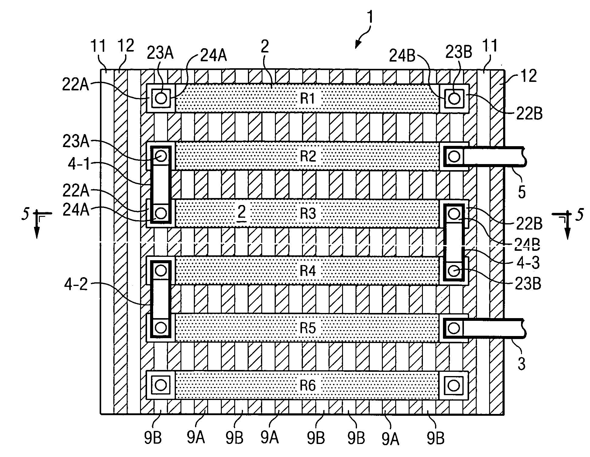
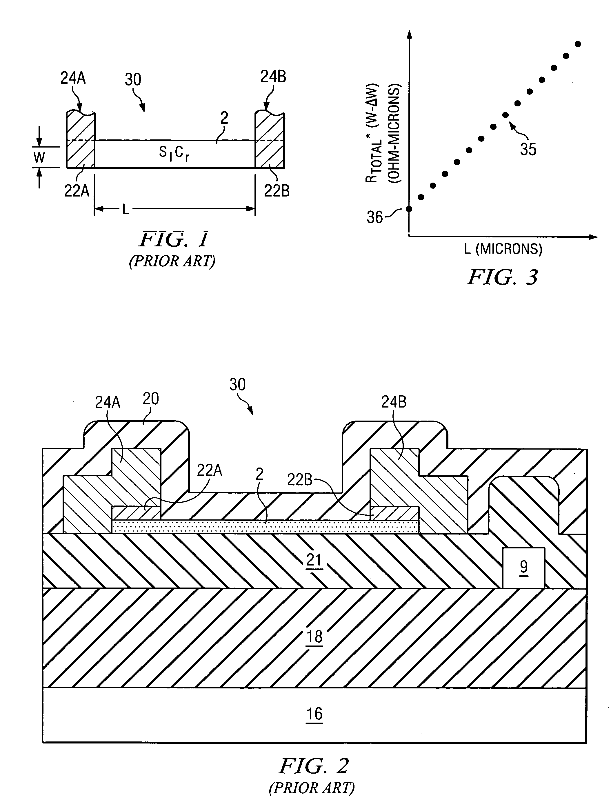
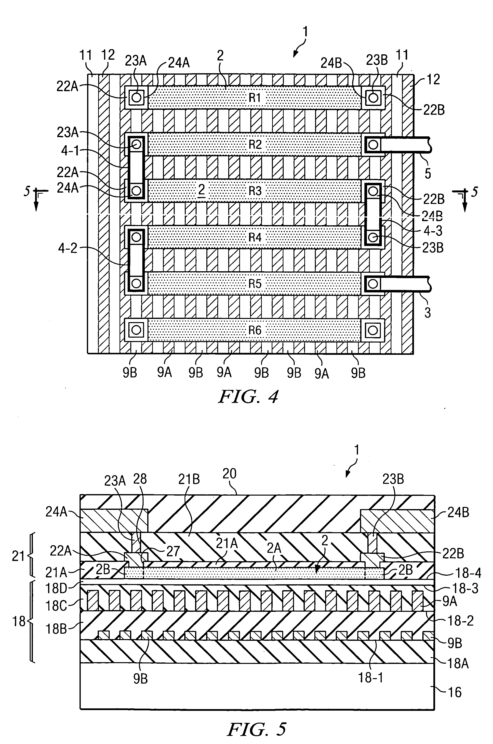
[0031] The present invention is directed mainly to head resistivity aspects of the accuracy of thin film resistors. For a high-resistance thin film resistor, the accuracy of the head resistance and head resistivity may not be highly significant, but if the value of the thin film resistor is very low, for example 160 ohms, and very high precision is needed, for example in manufacture of a high-resolution string DAC, the head resistance might be 5 ohms at each end of a 160 ohm string resistor. A high variance in the head resistivity of such a low-value, high-precision string resistor would be completely unacceptable if the main objective was to make a string DAC with 14-bit or higher resolution / accuracy. The following embodiment of the invention provides a structure and method for providing / manufacturing thin film resistors with very low variance of head resistivity.

[0032] Referring to FIG. 4, an experimental integrated circuit resistor structure is shown which includes generally the...


PUM


Abstract

A method of making integrated circuit thin film resistor includes forming a first dielectric layer (18B) over a substrate and providing a structure to reduce variation of head resistivity thereof by forming a dummy fill layer (9A) on the first dielectric layer, and forming a second dielectric layer (18D) over the first dummy fill layer. A thin film resistor (2) is formed on the second dielectric layer (18D). A first inter-level dielectric layer (21A) is formed on the thin film resistor and the second dielectric layer. A first metal layer (22A) is formed on the first inter-level dielectric layer and electrically contacts a portion of the thin film resistor. Preferably, the first dummy fill layer is formed as a repetitive pattern of sections such that the repetitive pattern is symmetrically aligned with respect to multiple edges of the thin-film resistor (2). Preferably, the first dummy fill layer is formed so as to extend sufficiently far beyond ends of the thin-film resistor to ensure only a negligible amount of systematic resistance error due to misalignment.

Description

BACKGROUND OF THE INVENTION [0001] The present invention relates generally to integrated circuit thin film resistors, and more particularly to a thin film resistor structure and method that provide very low variance in the head resistivity of thin film resistors. [0002]FIG. 1 shows a plan view of a prior art thin film resistor 30, which may be composed of, for example, sichrome (SiCr), designated by reference numeral 2. FIG. 2 shows a section view of thin film resistor structure 30 of FIG. 1. Referring to FIGS. 1 and 2, thin film resistive layer 2 of resistor structure 30 has an elongated rectangular configuration of width W, including a central body portion of length L and two identical “head” sections 22A and 22B contacted by metal conductors 24A and 24B, respectively. [0003]FIG. 2 shows an accurate section view of a portion of a prior art integrated circuit including a prior art thin film resistor structure in which a sichrome (SiCr) thin film resistor 2 formed on a layer or regi...

Claims


Application Information

Patent Timeline
Patent Type & Authority Applications(United States)
IPC IPC(8): H01L21/4763
CPCH01C7/006H01L28/20H01L23/5228H01C17/075H01L2924/0002H01L2924/00
Inventor BEACH, ERIC W.STEINMANN, PHILIPP
Owner TEXAS INSTR INC
Why Eureka
Try Eureka