Thin film resistor and dummy fill structure and method to improve stability and reduce self-heating

a thin film resistor and filling structure technology, applied in the direction of resistor details, semiconductor/solid-state device details, etc., can solve the problems of insufficient removal of undesired metallization residues, inability to meet many conventional integrated circuit processing steps, and inability to meet the requirements of non-planar surfaces, etc., to reduce the thermal resistance of silicon substrates, improve the structure of thin film resistors, and reduce the cost of integrated circuits.

Active Publication Date: 2008-07-22
TEXAS INSTR INC
View PDF2 Cites 17 Cited by
  • Summary
  • Abstract
  • Description
  • Claims
  • Application Information

AI Technical Summary

Benefits of technology

[0010]It is an object of the invention to provide an improved, inexpensive integrated circuit thin film resistor structure and method for reducing or eliminating inaccuracy in the resistances and ratios of the resistances of thin film resistors.
[0011]There also is an unmet need for an improved, inexpensive integrated circuit thin film resistor structure and method for reducing or eliminating inaccuracy in the ratios of resistances of thin film resistors having substantially different current densities therein.
[0012]It is another object of the invention to provide an improved, inexpensive integrated circuit thin film resistor structure and method for reducing self-heating of a thin film resistor by uniformly reducing thermal resistance to a silicon substrate.
[0013]It is another object of the invention to provide an improved, inexpensive integrated circuit thin film resistor structure and method providing improved nucleation of thin film resistive material on dielectric material on which the thin film resistive material is formed.
[0014]It is another object of the invention to provide an improved, inexpensive integrated circuit thin film resistor structure and method for improving nucleation of resistive material being deposited on damaged dielectric surfaces.

Problems solved by technology

Non-planar surfaces are incompatible with many conventional integrated circuit processing steps.
For example, if interconnect metallization is deposited on a non-planar surface and the resulting surface then is subjected to a CMP operation, there may be residues of undesired metallization which are not adequately removed.
Such undesired metallization residues may cause electrical shorting or other problems that lower integrated circuit processing yield.
When CMD operations are performed in the vicinity of thin film resistors, the “dishing” referred to above may cause large “systematic” errors in the resistances and ratio-matching of resistances of the thin film resistors.
Not only is the resistance of every identical resistor or resistor segment different for different die and different wafers, the systematic error associated with the resistor segments typically varies significantly even within the same die.
For prior art integrated circuit surface planarizing processes, it was considered unacceptable to have any metal or any other abrupt integrated circuit topology features located underneath thin film resistors.
This was because the prior art integrated circuit surface planarizing processes could not adequately planarize or precisely flatten such topology features well enough to avoid severe disruption of the matching and stability of the thin film resistors due to material stresses and / or discontinuities (especially in very thin layers such as SiCr which, for example, may be only about 30 Angstroms thick) and / or optical inaccuracies associated with photolithography techniques being used.

Method used


Image

  • Thin film resistor and dummy fill structure and method to improve stability and reduce self-heating
  • Thin film resistor and dummy fill structure and method to improve stability and reduce self-heating
  • Thin film resistor and dummy fill structure and method to improve stability and reduce self-heating

Examples


Embodiment Construction

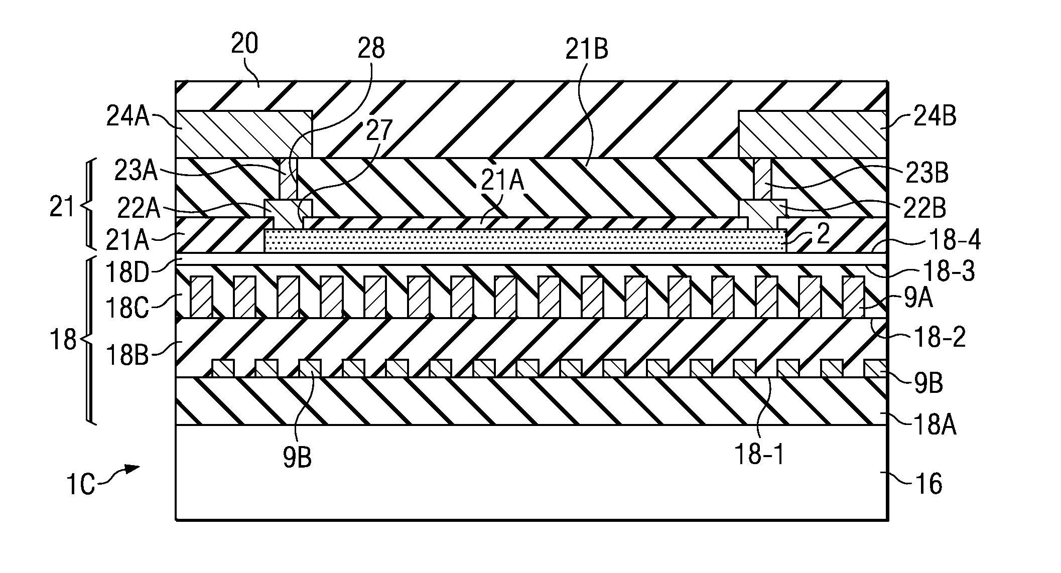
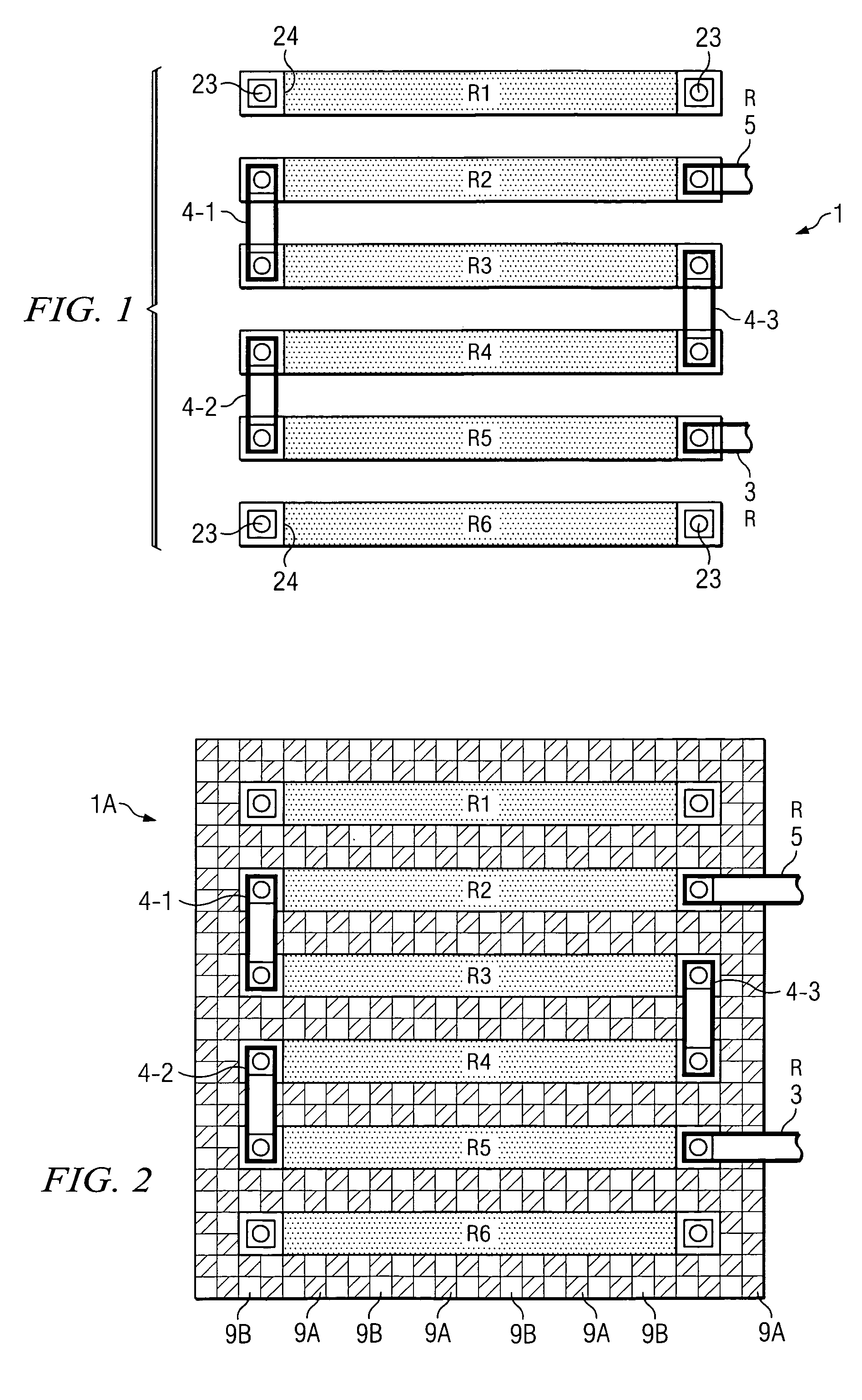
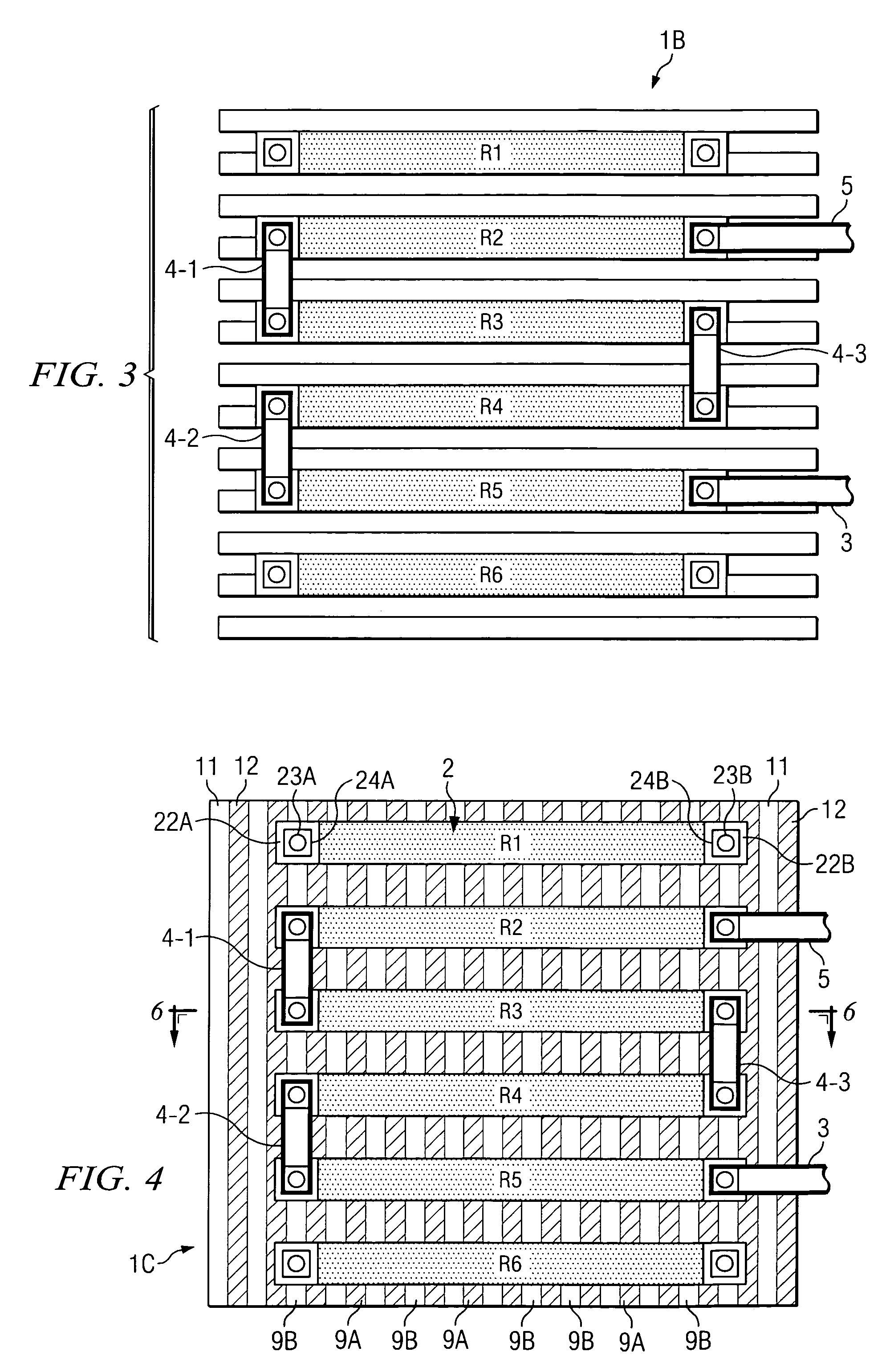
[0024]FIG. 1 shows a plan view of an integrated circuit resistor structure 1 including elongated, rectangular resistive film segments or resistors R1,2 . . . 6 composed of thin film material such as SiCr (sichrome). The segments R1,2 . . . 6 all are essentially identical in length, width, and spacing between the segments. A metal terminal 5 is connected through a tungsten via or plug 23 to a thin film resistor “head”24 of thin film resistor segment R2. Thin film resistor head 24 typically is composed of TiN (titanium-nitride). The left end of resistor segment R2 is connected in the same manner to one end of a metal connector 4-1, the other end of which is connected through a tungsten plug and a TiN head to the left end of resistor segment R3, the right end of which is connected by metal connector 4-3 to the right end of resistor segment R4. Similarly, segments R4 and R5 are connected in series with segments R3 and R4 and with terminals 3 and 5 to form a “composite” thin film resisto...


PUM


Abstract

An integrated circuit thin film resistor structure includes a first dielectric layer (18A) disposed on a semiconductor layer (16), a first dummy fill layer (9A) disposed on the first dielectric layer (18B), a second dielectric layer (18C) disposed on the first dummy fill layer (9A), the second dielectric layer (18B) having a first planar surface (18-3), a first thin film resistor (2) disposed on the first planar surface (18-3) over the first dummy fill layer (9A). A first metal interconnect layer (22A,B) includes a first portion (22A) contacting a first head portion of the thin film resistor (2). A third dielectric layer (21) is disposed on the thin film resistor (2) and the first metal interconnect layer (22A,B). Preferably, the first thin film resistor (2) is symmetrically aligned with the first dummy fill layer (9A). In the described embodiments, the first dummy fill layer is composed of metal (integrated circuit metallization).

Description

BACKGROUND OF THE INVENTION[0001]The present invention relates generally to semiconductor devices and techniques for providing dummy fill structures beneath thin film resistors that preferably are symmetric with respect to the thin film resistors, so as to reduce self-heating, preferably uniformly, of the thin film resistors and improve the stability of the thin film resistors, especially the stability of ratios of resistances of thin film resistors having different current densities therein.[0002]“Dummy fill” has been commonly utilized in conjunction with use of chemical mechanical polishing (CMP) in integrated circuit chip fabrication processes. Dummy fill also has been utilized beneath an array of thin film resistors to disperse laser beam energy reflected during trimming of the thin film resistors so as to reduce optical interference of reflected laser energy with the incident laser beam and thereby improve laser trimming of the thin film resistors, as described in commonly assi...

Claims


Application Information

Patent Timeline
Patent Type & Authority Patents(United States)
IPC IPC(8): H01C1/012
CPCH01L23/5228H01L28/20H01L27/016H01L2924/0002H01L2924/00
Inventor BEACH, ERIC W.MEINEL, WALTER B.STEINMANN, PHILIPP
Owner TEXAS INSTR INC
Why Eureka
Try Eureka