Structure and method for minimizing substrate effect on nucleation during sputtering of thin film resistors

a thin film resistor and nucleation effect technology, applied in the field of semiconductor structure, can solve the problems of chemical bonding, damage, damage, etc., and achieve the effects of avoiding surface damage, improving the nucleation of material being deposited, and inexpensive integrated circuit thin film resistor structur

Inactive Publication Date: 2006-10-12
TEXAS INSTR INC
View PDF1 Cites 2 Cited by
  • Summary
  • Abstract
  • Description
  • Claims
  • Application Information

AI Technical Summary

Benefits of technology

[0020] It is another object of the invention to provide an inexpensive integrated circuit thin film resistor structure and method which avoids the effects of surface damage caused by prior techniques for removing or mitigating surface damage on dielectric layer surfaces on which thin film material is to be deposited.
[0021] It is another object of the invention to provide an improved, inexpensive integrated circuit thin film resistor structure and method for improving nucleation of material being deposited on abraded or otherwise damaged dielectric surfaces.
[0022] Briefly described, and in accordance with one embodiment, the present invention provides a method of improving nucleation during depositing of a film (2) on a surface (18-3) of a wafer, including performing a planarizing operation on the surface (18-3), the planarizing operation resulting in generation of dangling chemical bonding s

Problems solved by technology

A chemically/mechanically polished oxide surface always has an abraded and therefore damaged surface.
(The damage also may be caused by a prior etching process such as a prior “etch back” process or a prior cleaning process such as a “sputter clean” process.
Also, damage may be caused by a cleanup etching to remove slurry utilized in the chemical/mechanical polishing process.)
Although the chemically/mechanically polished oxide surface 30 is very smooth, at an atomic level it is damaged such that there are chemical bonds that are not “passified” or “passivated”.
Therefore, the nonhomogeneous film of SiCr will have unpredictable, random resistivity variations therein and unpredictable, random variations in its sheet resistance.
There is an important relationship of the amorphous film structure to the amorphous substrate structure that affects growth of the film being deposited, and that relationship is not sufficiently well-controlled if there is damage or residue on the substrate at the onset of deposition of the film.
Defective nucleation sites on the substrate surface due to such damage are significant factors affecting the film deposition and the electrical properties of the resulting film.
This makes it difficult for the manufacturing process to meet a particular target sheet resistance specification for the resulting SiCr layers, and there will be a large variance in th

Method used


Image

  • Structure and method for minimizing substrate effect on nucleation during sputtering of thin film resistors
  • Structure and method for minimizing substrate effect on nucleation during sputtering of thin film resistors
  • Structure and method for minimizing substrate effect on nucleation during sputtering of thin film resistors

Examples


Embodiment Construction

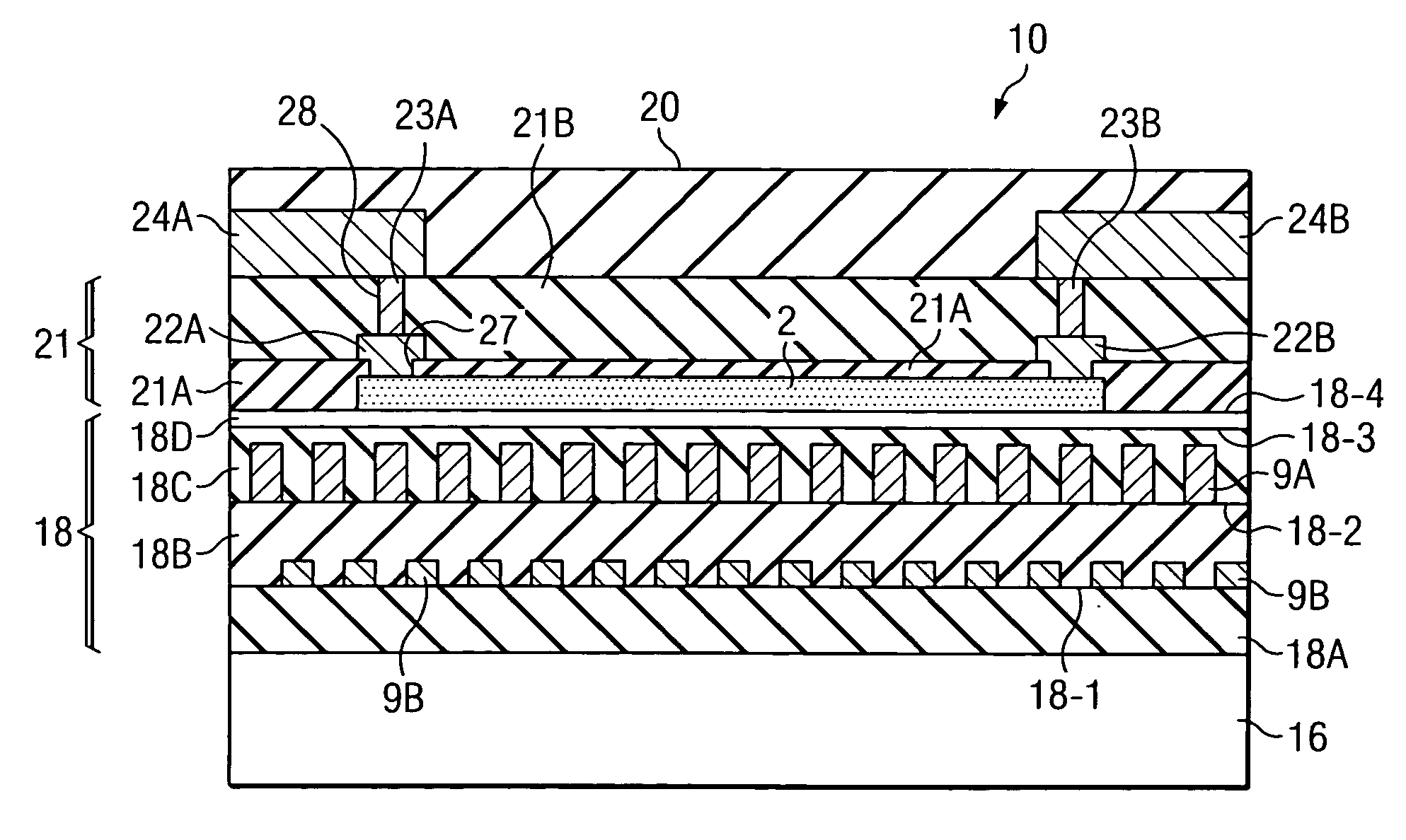
[0033] Referring to FIG. 9, pre-metal dielectrics region 18 is formed on silicon substrate 16, which could be an epitaxial silicon layer formed directly on a semiconductor wafer. Region 18 includes a dielectric layer 18A formed on the upper surface of silicon layer 16. An arrangement of optional parallel polycrystalline silicon strips 9B can be formed on the upper surface 18-1 of dielectric layer 18A to form a first dummy fill layer, and another dielectric layer 18B is formed on surface 18-1 of dielectric layer 18A and the first dummy fill layer 9B. A layer of spaced metallization strips 9A and / or other metallization interconnect pattern (not shown) forms an optional second dummy fill layer on a chemically / mechanically polished surface 18-2 of dielectric layer 18B. A dielectric layer 18C is formed on surface 18-2 of dielectric layer 18B and the metallization pattern 9A. The upper surface 18-3 of dielectric layer 18C is planarized by a conventional chemical / mechanical polishing proce...


PUM

PropertyMeasurementUnit
Lattice constantaaaaaaaaaa
Thicknessaaaaaaaaaa
Thicknessaaaaaaaaaa

Abstract

A method of improving nucleation during depositing of a film (2) on a surface (18-3) of a wafer, including performing a planarizing operation on the surface (18-3), the planarizing operation resulting in generation of dangling chemical bonding sites on the surface, depositing a dielectric layer (18D) on the planarized surface (18-3) to cover the dangling chemical bonding sites to thereby produce a more uniform surface for nucleation of subsequently deposited resistive film material, and depositing a film (2) of resistive material on the dielectric layer (18D), whereby more uniform nucleation results in the film (2) being very uniform. The film of resistive material is deposited on the dielectric layer directly after the depositing of the dielectric layer, without any further treatment of the dielectric layer (18D).

Description

BACKGROUND OF THE INVENTION [0001] The present invention relates generally to semiconductor structures and techniques for providing improved nucleation for deposition of one amorphous layer on another amorphous layer, and more particularly for deposition of thin film resistive materials on chemically / mechanically polished (CMP) or otherwise damaged surfaces of dielectric layers. [0002]FIG. 1 shows a section view of a portion of a prior art integrated circuit including a thin film resistor structure in which a SiCr (sichrome) thin film resistor 2 is formed on an “interlevel dielectrics” region or layer 21 which may include several conventional dielectric layers (not shown). Layer 21 is formed on a “pre-metal dielectrics” or oxide layer 18 which is formed on a silicon layer 16. (The term “pre-metal dielectrics” is well-known in the integrated circuit industry, and refers to contiguous pre-metal dielectric layers having somewhat different doping, including for example, boron-phosphorus...

Claims


Application Information

Patent Timeline
IPC IPC(8): H01L21/4763H01L21/31H01L21/469
CPCH01L28/24C23C14/024
Inventor BEACH, ERIC W.
Owner TEXAS INSTR INC
Why Eureka
Try Eureka