
Systems and methods for wiring circuit components

Inactive Publication Date: 2006-10-19
KK TOSHIBA
View PDF5 Cites 3 Cited by
  • Summary
  • Abstract
  • Description
  • Claims
  • Application Information

AI Technical Summary

Benefits of technology

[0009] One or more of the problems outlined above may be solved by the various embodiments of the invention. Broadly speaking, the invention includes systems and methods for arranging parallel wires to reduce the capacitance variations among the wires and to thereby reduce the skew of the signals on the different wires and the time required for signals to traverse the wires.

Problems solved by technology

Decreasing the size of these components, however, can result in problems that prevent the devices from operating more quickly, and may even cause the devices to malfunction.
The increased coupling capacitance in turn results in increased interference between the wires.
Additionally, as the complexity of the electronic circuits increases, longer wires (and more widely varying lengths of wires) may be necessary to connect individual components within the circuit.
This is problematic in circuits which couple signals from a large number of components into another component because it is difficult to keep the signal paths the same length.
As a result, it may take different amounts of time for the signals to reach the end component, and the phases of the signals may consequently become skewed with respect to each other.
Further, because the capacitance is greatest in the longest signal lines, the increased time necessary to traverse the longest signal lines forces the circuits to be operated at slower speeds.
The problem with these conventional solutions to the problem is that, by increasing the width of the wires or by increasing the spacing between the wires, the size of the circuit is increased.
This goes against the desired reductions in size.

Method used


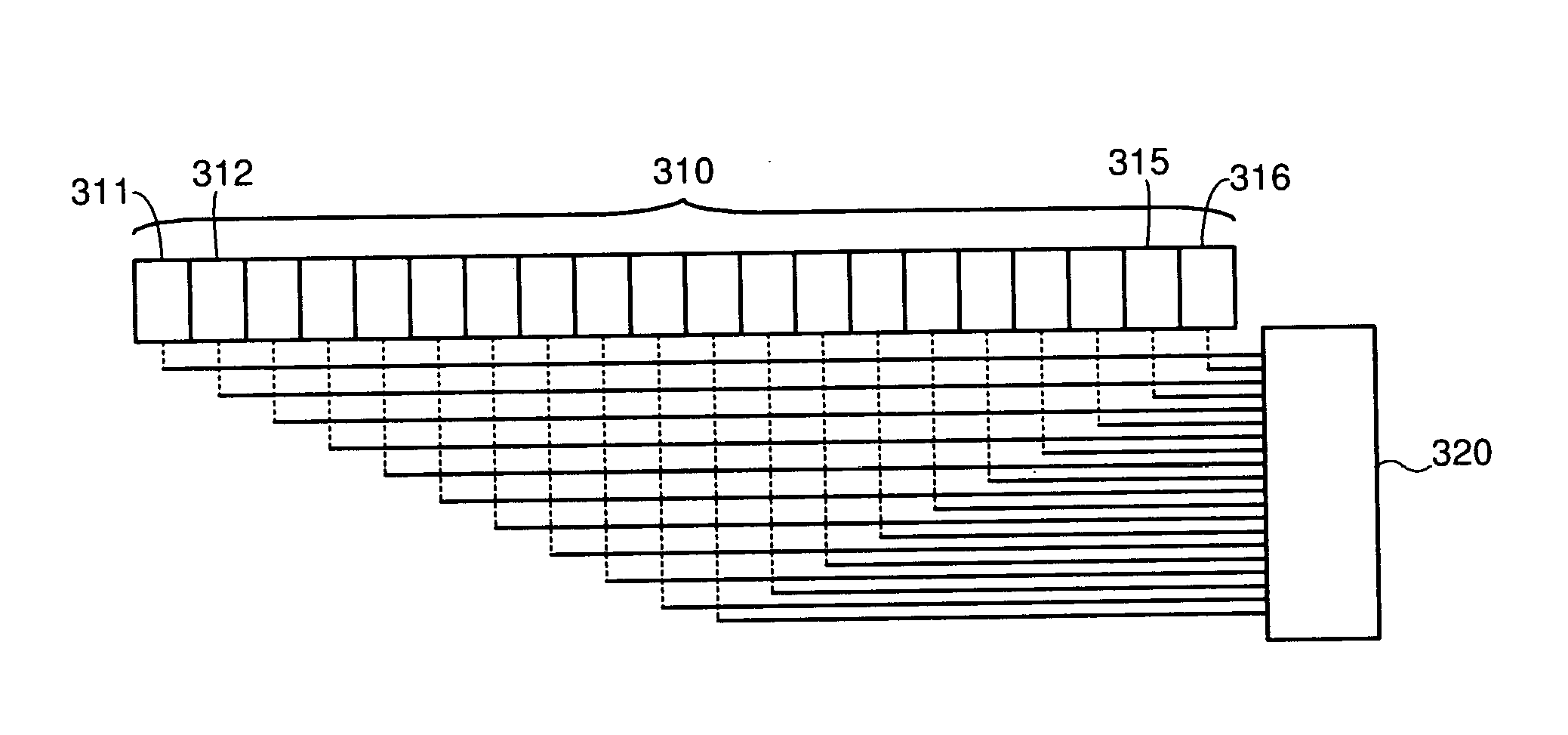
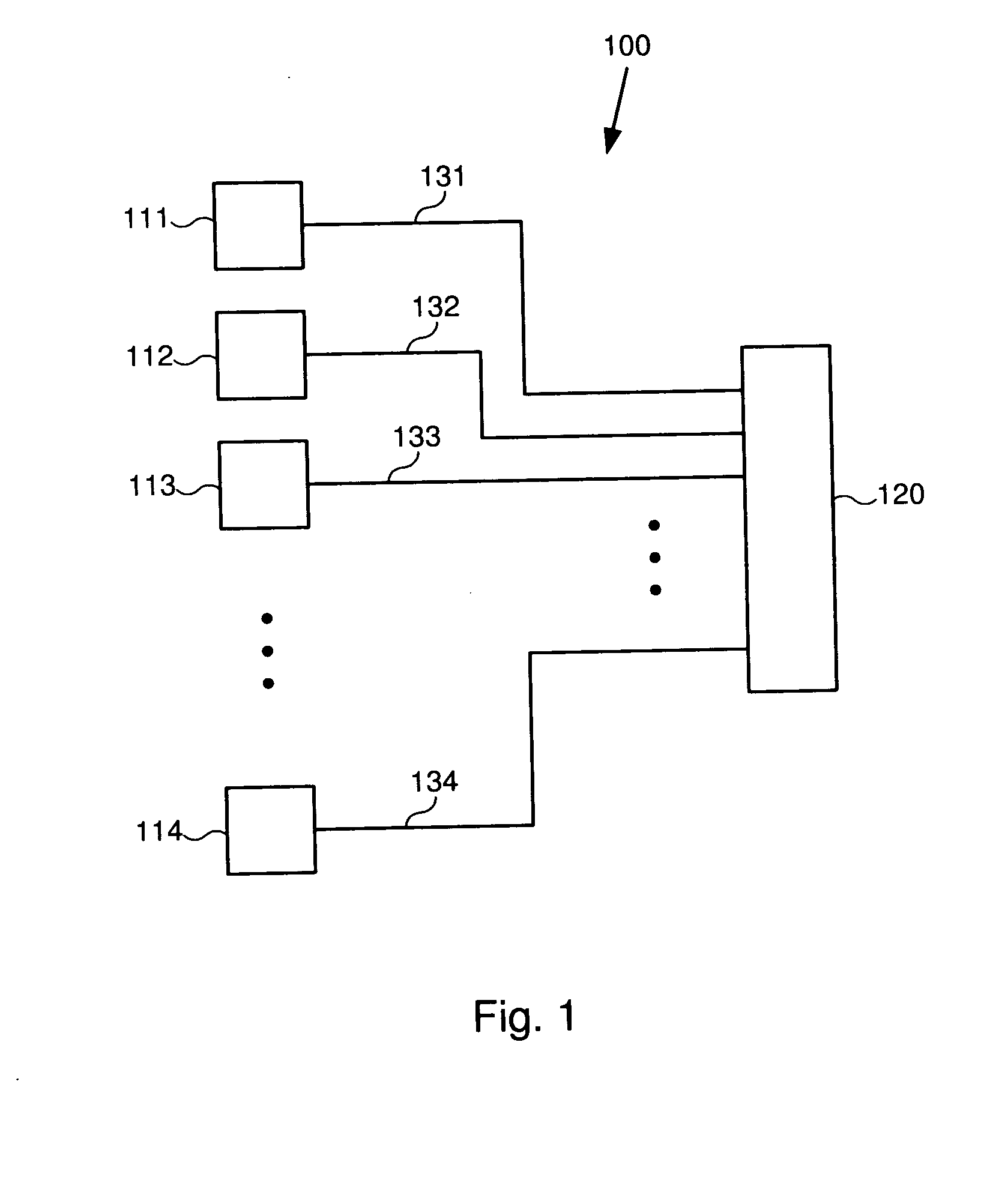
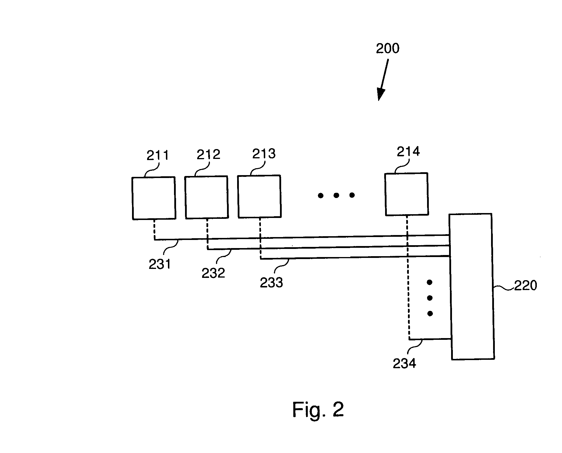
Image

  • Systems and methods for wiring circuit components
  • Systems and methods for wiring circuit components
  • Systems and methods for wiring circuit components

Examples


Embodiment Construction

[0023] One or more embodiments of the invention are described below. It should be noted that these and any other embodiments described below are exemplary and are intended to be illustrative of the invention rather than limiting.

[0024] Broadly speaking, the invention includes systems and methods for arranging parallel wires to reduce the capacitance variations among the wires and to thereby reduce the skew of the signals on the different wires and the time required for signals to traverse the wires.

[0025] In one embodiment, multiple first components, such as buffers or latches are coupled to a second component, such as an encoder, or error correction logic. The first components are physically arranged as a linear array. The second component is positioned at the end of this linear array. Each of the first components is coupled to the second component by a wire that has a perpendicular portion extending perpendicular to the direction of the linear array, and a parallel portion which...


PUM


Abstract

Systems and methods for arranging parallel wires to reduce the capacitance variations. In one embodiment, multiple first components arranged as a linear array are coupled to a second component at the end of this linear array by corresponding signal wires. Each signal wire has a perpendicular portion extending perpendicular to the direction of the linear array, and a parallel portion which runs parallel to the direction of the linear array. The parallel portions are staggered so that longer ones of the parallel portions are adjacent to the shorter ones of the parallel portions, instead of simply being arranged from longest to shortest. In one embodiment, the longer half of the parallel portions decrease in length across the series of parallel portions, while the shorter half of the parallel portions increase in length. In another embodiment, successively longer / shorter parallel portions alternate sides of the series.

Description

BACKGROUND [0001] 1. Field of the Invention [0002] The invention relates generally to electronic circuits, and more particularly to systems and methods for laying out wiring between a first set of circuit components and a second component. [0003] 2. Related Art [0004] With advancements in electronics technology, there is constantly a demand for improved electronic devices. Aside from the demand for new features in these devices, there is a demand to make the same devices smaller and faster. In order to make electronic devices smaller and faster, it is normally necessary to make the components that form the devices physically smaller. Decreasing the size of these components, however, can result in problems that prevent the devices from operating more quickly, and may even cause the devices to malfunction. [0005] As the size of electronic components decreases, the size and spacing (pitch) of the wires connecting these components also decreases. As the pitch of the wires in an electric...

Claims


Application Information

Patent Timeline
IPC IPC(8): G06F17/50
CPCG06F17/5068G06F30/39
Inventor MAKINO, EIICHI
Owner KK TOSHIBA
Learn More