NAND flash memory management

a technology memory management, applied in the field of electronic devices, can solve the problems of nand flash memory, low power consumption, and small size of flash memory devices, and achieve the effects of low power consumption, low cost, and low cos

Active Publication Date: 2006-10-26
MICROSOFT TECH LICENSING LLC
View PDF3 Cites 341 Cited by
  • Summary
  • Abstract
  • Description
  • Claims
  • Application Information

AI Technical Summary

Problems solved by technology

Flash memory devices are typically small, light weight, and consume low amounts of power.
However, NAND flash memory has a disadvantage which, to date, has limited its use.
NAND flash memory is prone to developing bad blocks of memory.
One observance is that blocks within a NAND flash memory device are bad when the NAND flash memory device is delivered from the manufacturer.
The other is that blocks go bad while the NAND flash memory device is being used.

Method used


Image

  • NAND flash memory management
  • NAND flash memory management
  • NAND flash memory management

Examples


Embodiment Construction

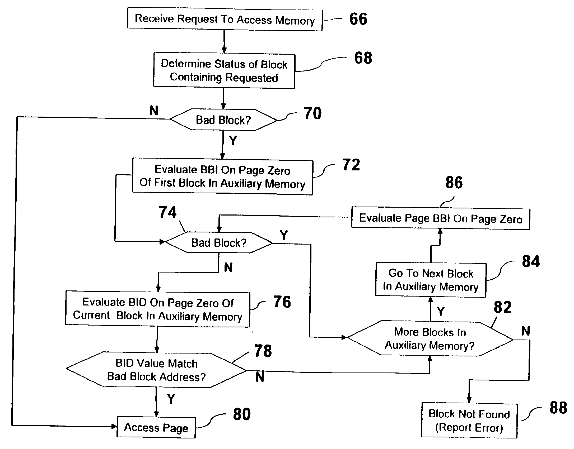
[0019] A memory management system is described herein with application to NAND flash memory. However, it is to be understood that the application of this memory management system should not be limited thereto. This memory management system is applicable to any appropriate type of memory, such a NAND flash memory, NOR flash memory, flash memory in general, non-flash memory, or a combination thereof, for example.

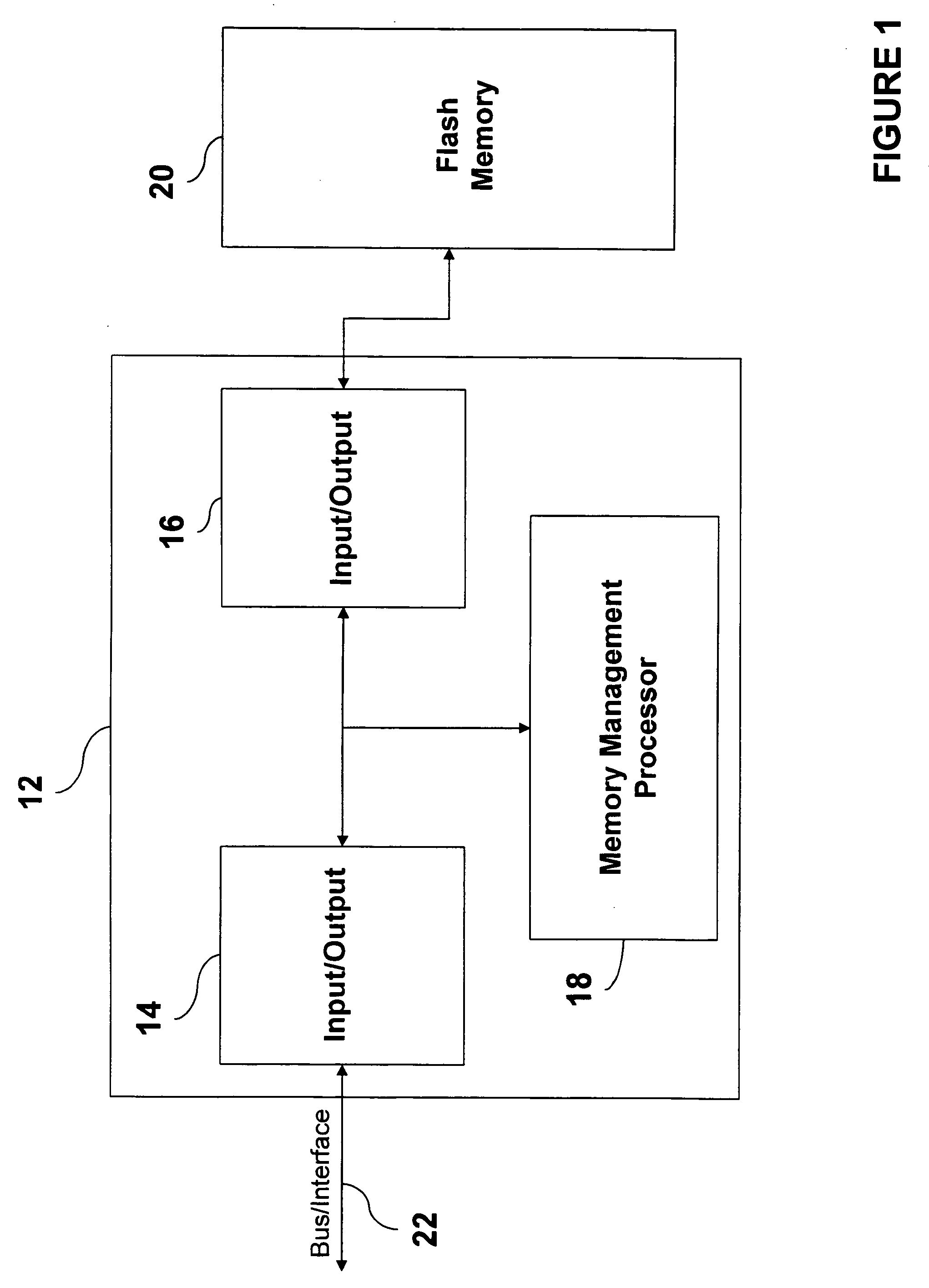
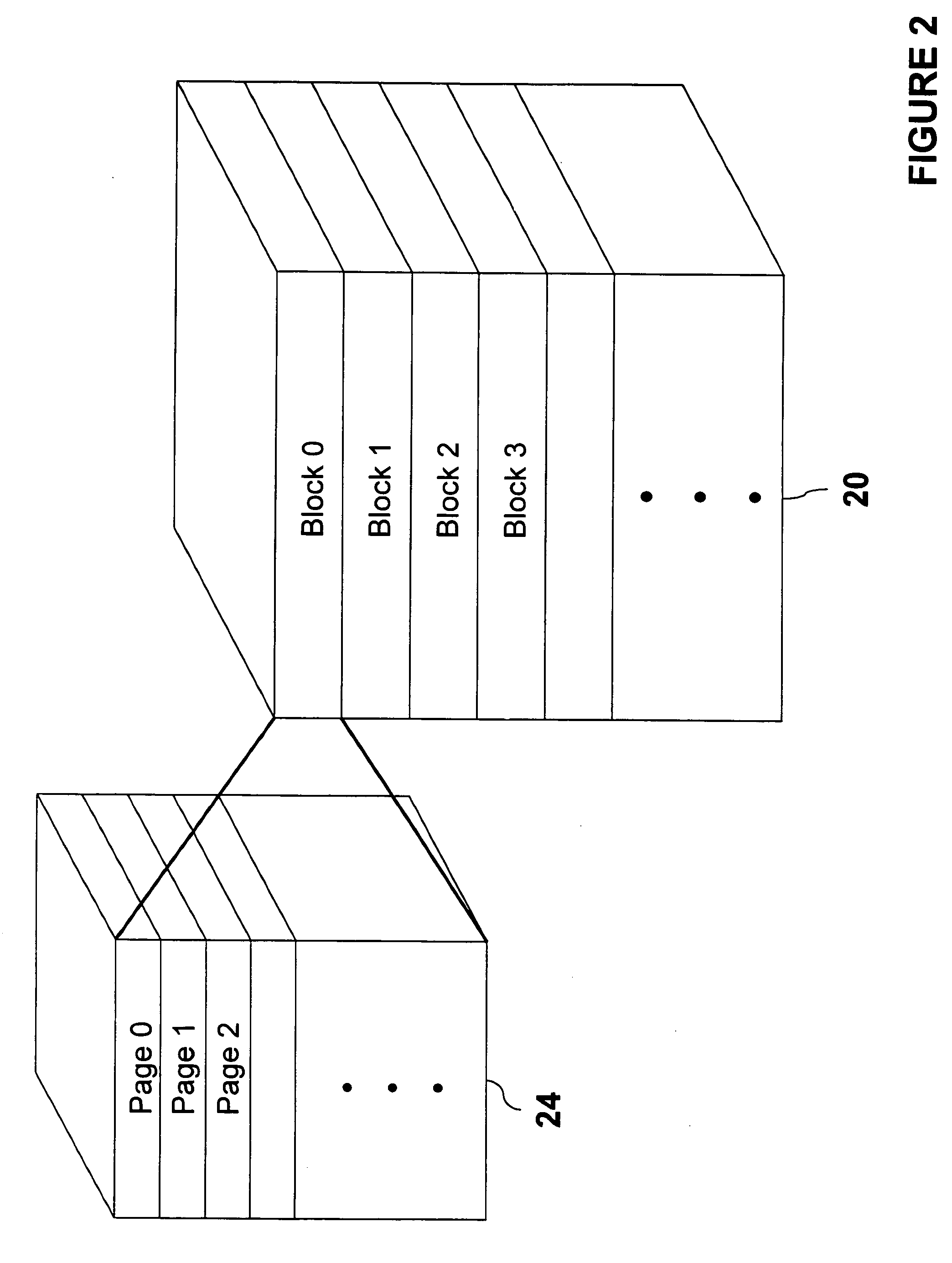
[0020]FIG. 1 is a diagram of a memory management system comprising memory controller 12 and NAND flash memory device 20 in accordance with an exemplary embodiment of the present invention. The memory controller 12 comprises an input / output portion 14, an input / output portion 16, and a memory management processor 18. The input / output portion 14 is coupleable to any appropriate device desiring access (accessing device not shown in FIG. 1) to the NAND flash memory 20. The accessing device is coupled to the memory controller 12 via interface 22. The interface 22 can comprise any ...


PUM


Abstract

A memory controller is utilized to overcome NAND flash memory's propensity for comprising bad blocks of memory. The memory controller utilizes minimal hardware and is essentially transparent to a device requesting access to the NAND memory. A NAND flash memory device is configured to comprise a set of main blocks of memory and a set of auxiliary blocks of memory. Each block is divided into pages of memory and each page includes metadata. The metadata includes a block status indicator, indicating whether a block is good or bad. When receiving a request to access a page in the NAND flash memory, if the block in which the page resides is good, that block is accessed. If the block is bad, auxiliary memory is searched until a block containing the address of the bad block in its metadata is found. The found block is accessed in lieu of the bad block.

Description

FIELD OF THE INVENTION [0001] The present invention relates generally to electronics and specifically to memory management. The invention relates even more specifically to memory management of NAND flash memory devices. BACKGROUND OF THE INVENTION [0002] Flash memory is a form of electrically erasable programmable read only memory (EEPROM). Unlike typical EEPROM, which is erasable one byte at a time, flash memory is capable of being erased one block at a time. Block sizes vary for various flash memory devices. Flash memory devices are typically small, light weight, and consume low amounts of power. Thus, flash memory is appropriate for devices such as mobile devices, battery powered devices, devices desiring low power consumption, and / or small devices, for example. Two popular types of flash memory are NOR flash memory and NAND flash memory. As the names suggest, NOR flash memory utilizes circuitry comprising NOR gates and NAND flash memory utilizes circuitry comprising NAND gates. ...

Claims


Application Information

Patent Timeline
Patent Type & Authority Applications(United States)
IPC IPC(8): G11C16/04
CPCG06F12/0246G11C2216/14G11C29/76G11C16/10
Inventor WILLIAMS, GREGORY G.SINGH, HARJITLOVE, MICHAEL G.AU, STEPHEN Z.
Owner MICROSOFT TECH LICENSING LLC
Why Eureka
Try Eureka