Method for testing a memory chip and test arrangement

a memory chip and test arrangement technology, applied in the direction of digital storage, measurement devices, instruments, etc., can solve the problems of difficult simulation and precise identification of errors that occurred in practical application within the test system, and the speed of the overall system can be greatly influenced by algorithms,

Inactive Publication Date: 2007-09-18
POLARIS INNOVATIONS LTD
View PDF11 Cites 69 Cited by
  • Summary
  • Abstract
  • Description
  • Claims
  • Application Information

AI Technical Summary

Benefits of technology

[0016]The invention is directed to a method for testing a memory chip used for error correction which enables a precise identification of an error address. Moreover, the invention is further directed to an arrangement which enables a rapid identification of a defective memory cell in a simple fashion.
[0025]Preferably, data are then written to memory cells of the at least one memory chip and of the memory chip provided for the error correction data. This embodiment of the invention makes it possible to detect even errors that occur dynamically and in a manner dependent on data contents within the memory chip provided for the error correction data and to identify an unambiguous addressing of the defective memory cells or the precise location of the error by means of the address thereof. This is possible in the course of operation of a test program that is situated in another memory module and is executed on the computer, and may be effected for example not only in a special test mode with special test data but also with normal application or program data. As a result, it is possible to map realistic scenarios and to react in a customized manner to problems that occur.
[0029]The test arrangement according to the invention enables extensive realistic test scenarios in the course of operation of a computer system. The control device monitors and controls the signal flow between the first and second interfaces in a suitable manner, so that an erroneous operation is avoided.
[0033]In one embodiment of the invention, the test memory chip is coupled to the second interface in disconnectable fashion via a first switching device, which can be controlled by the control device. As a result, the test memory chip can preferably be disconnected from the corresponding signal lines and thus also from the second interface. This embodiment is particularly expedient during a read process in a normal operating mode since an erroneous read-out of error correction data is thus avoided. In one development of the invention, the test memory chip is coupled to the at least one signal line, the at least one signal line being provided for an exchange of error correction data between the first interface and the second interface and thus between the memory controller of a computer system and the memory chip of the memory module that is provided for error correction data.
[0035]In another embodiment of the invention, a second switching device is provided, which can be controlled by the control device and is connected between the first and the second interface. Preferably, the second switching device is configured, in the first operating state, to connect the first interface to the second interface and, in the second operating state, interrupt the first interface with the second interface. What is thereby achieved is that, in the second operating state, a memory control device connected to the first interface does not receive any signals and the control device of the test arrangement can be put into the second operating state in a manner free of errors.

Problems solved by technology

In this context, the importance of test sequences and test methods for discovering possible errors is increasing since a failure on account of a hardware fault or else a design error, due to the high complexity of the memory chips used, cannot be ruled out from the outset in the design phase.
However, said algorithms can greatly influence the speed of the overall system and in particular of read and write processes in the memory and are therefore not usually published by the manufacturers of the memory controllers.
If an error occurs, the memory controller reports an error, an “ECC fail event”, to a main processor of the computer system.
In the case of such a message, however, it is not possible for the processor or a test program to ascertain whether the error occurred within the memory cell of one of the memory chips B1 to B8 or within the correction memory chip ECC.
In practice, however, it proves to be difficult to simulate and precisely identify the errors that occurred in practical application within the test system.
This results from ignorance of the algorithm used for the generation of error correction data of a memory controller.
During a test within a test system, both static and dynamic errors occur, which can be assigned to the specific error only with difficulty.
In this case as well, however, the data which a memory controller writes to the error correction memory are not known in advance.
As a result, an error that depends on the data content of the memory cells or electrical parameters might no longer be demonstrable.

Method used


Image

  • Method for testing a memory chip and test arrangement
  • Method for testing a memory chip and test arrangement
  • Method for testing a memory chip and test arrangement

Examples


Embodiment Construction

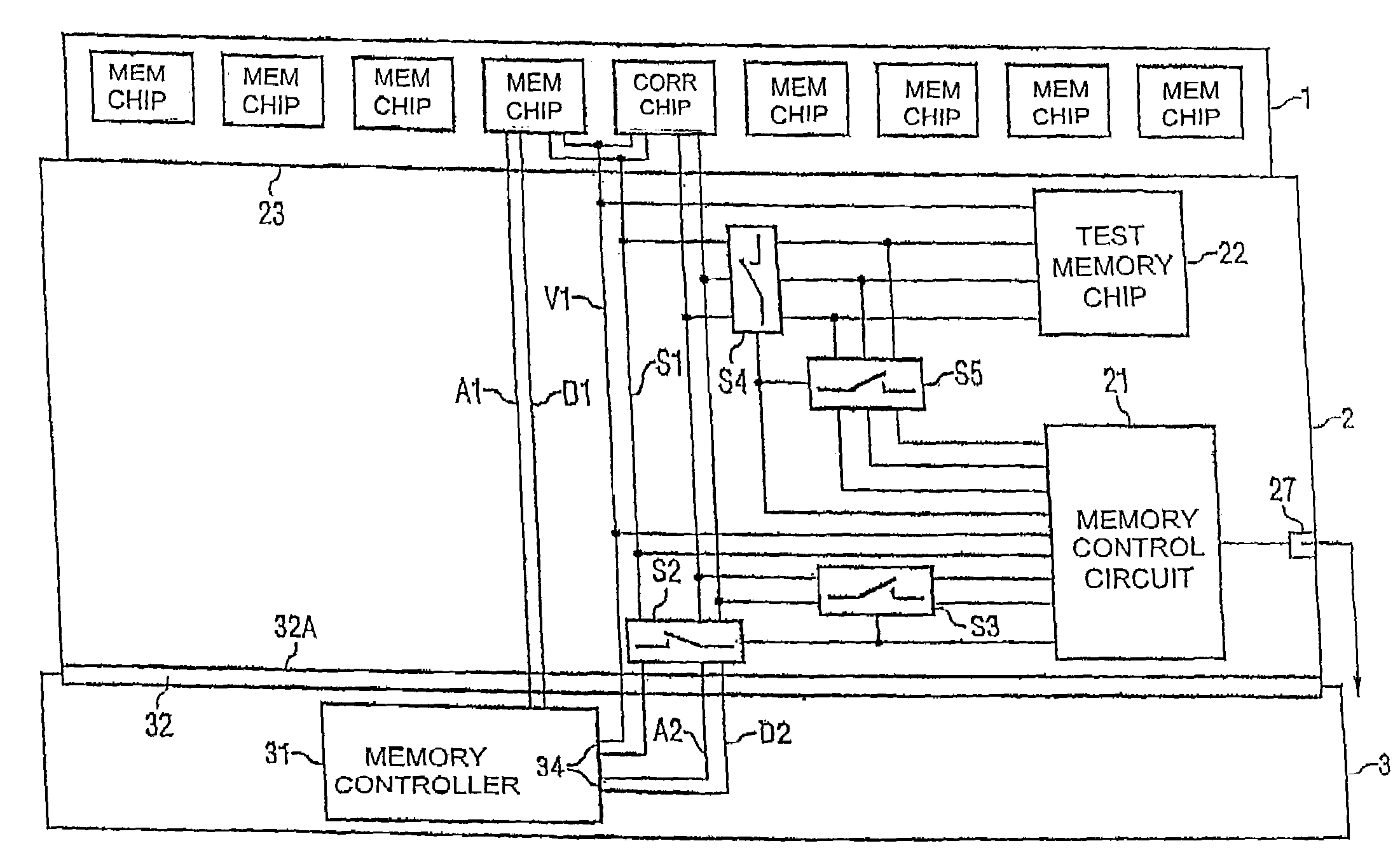
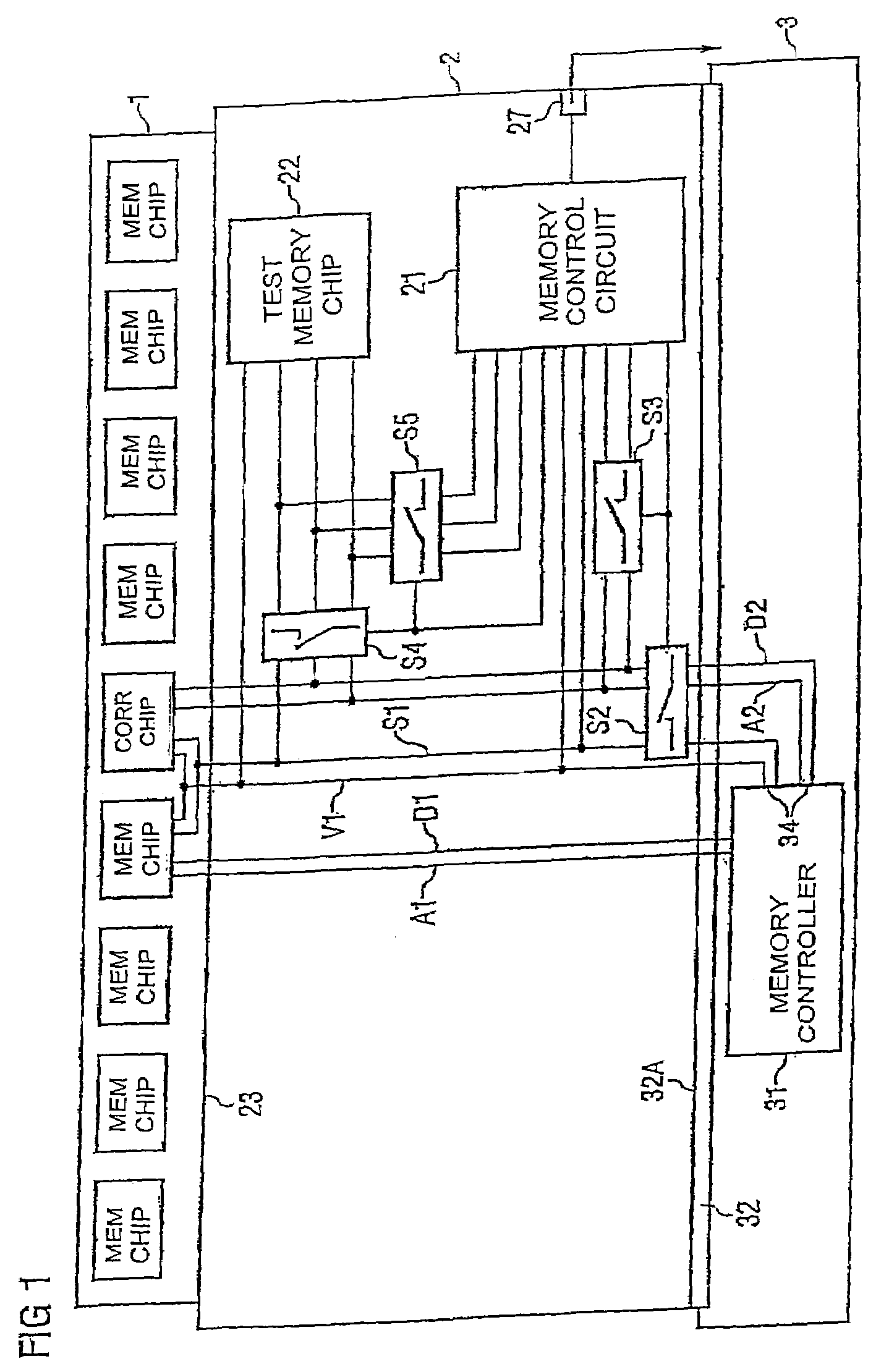
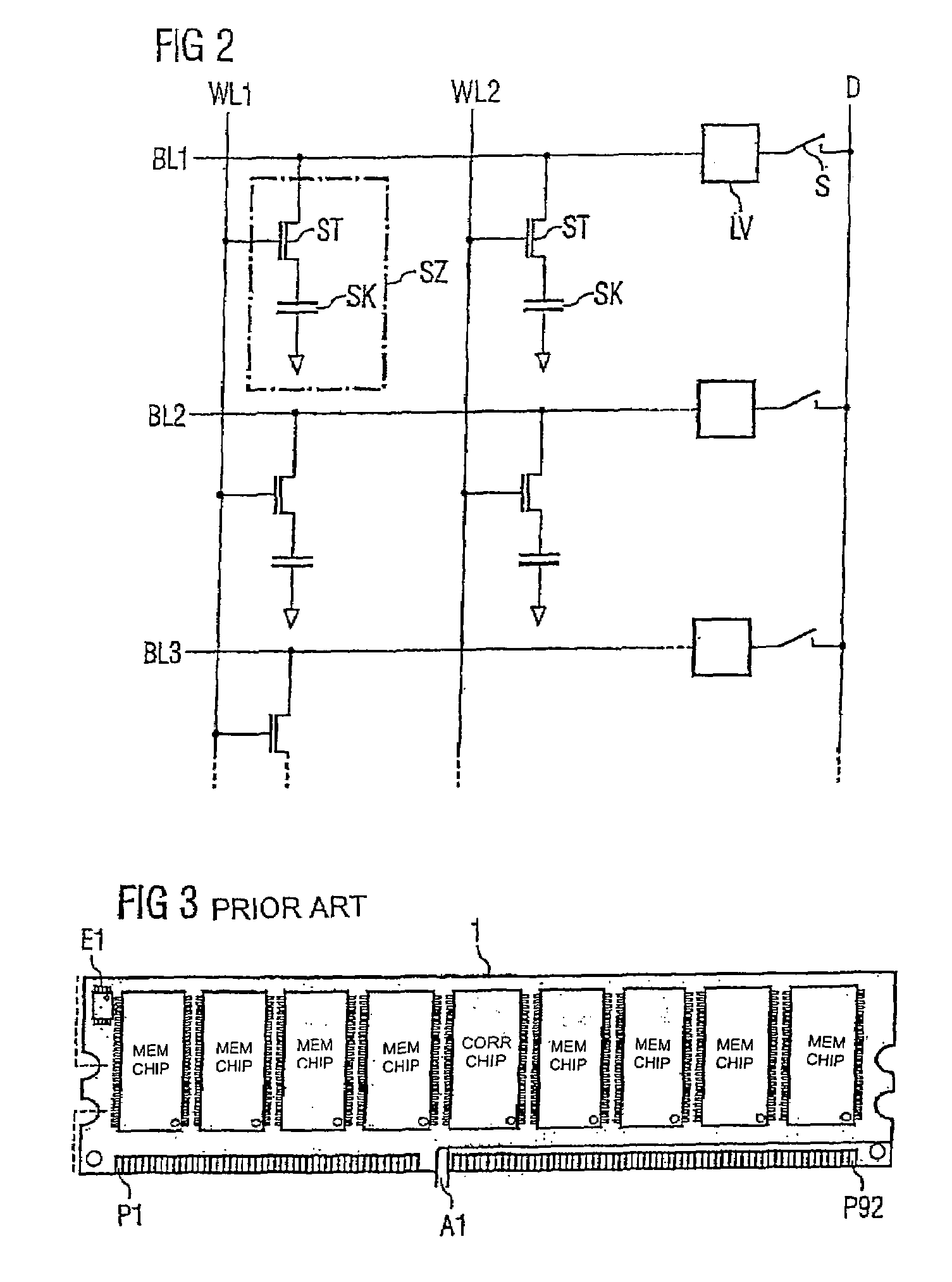
[0046]FIG. 3 shows a known exemplary embodiment of a memory module 1 that is inserted into a memory module slot of a computer system. A memory controller arranged within the computer system (not illustrated here) serves for control and also for addressing of memory cells to which data can be written or from which data can be read. For this purpose, the memory module 1 has a plurality of individual memory chips B1 to B8 which, for their part, contain a multiplicity or plurality of different memory cells.

[0047]Each of said memory chips B1 to B8 is for its part connected to a number of pins P1 to P92. In this case, some of said pins carry address signals for addressing individual memory cells within one of the memory chips B1 to B8, while others serve for supply with a supply current or a supply voltage. Further pins are provided as data lines that carry the content of memory cells from the memory chips.

[0048]The memory controller, which is not illustrated for reasons of clarity, contr...


PUM


Abstract

A test arrangement with a test memory chip and a control device is provided. Error correction data are stored in the test memory chip with the aid of the control device. In the case of an error event, it is ascertained whether the error occurred on the error correction chip. If so, the memory controller compares the data stored in the error correction chip with the data of the auxiliary memory. The address of the error correction chip can be deduced from the address of the auxiliary memory, thereby enabling unambiguous addressing of a defective memory cell of the error correction chip.

Description

REFERENCE TO RELATED APPLICATIONS[0001]This application claims the benefit of the priority date of German application DE 10 2004 021 267.8, filed on Apr. 30, 2004, the contents of which are herein incorporated by reference in their entirety.FIELD OF THE INVENTION[0002]The invention relates to a method for testing a memory chip and to a test arrangement for the error analysis of at least one memory chip of a memory.BACKGROUND OF THE INVENTION[0003]A volatile main memory for computer systems, which is referred to in shortened form as RAM memory module, is of great importance in modern computer systems. Advancing technology and the simultaneous fall in prices permit the use of memory modules with a multiplicity of individual memory chips fitted thereon up to a total capacity of 2 GB even in small personal computer systems. Larger storage capacities are continually being developed. In this context, the importance of test sequences and test methods for discovering possible errors is incr...

Claims


Application Information

Patent Timeline
Patent Type & Authority Patents(United States)
IPC IPC(8): G11C21/00G11C29/00G11C29/42
CPCG11C29/42
Inventor STOCKEN, CHRISTIAN
Owner POLARIS INNOVATIONS LTD
Why Eureka
Try Eureka