Defect mitigation in display panels

a technology for display panels and defects, applied in the field of display panels, can solve the problems of high cost, difficult production of perfect panels, and high production costs, and achieve the effect of reducing the probability of having a class 3 panel of 1024768 resolution, and reducing the cost of production

Inactive Publication Date: 2006-11-02
WISTRON CORP
View PDF2 Cites 26 Cited by
  • Summary
  • Abstract
  • Description
  • Claims
  • Application Information

AI Technical Summary

Benefits of technology

[0005] Defect mitigation in display panels is accomplished by mapping pixel defects in panels, associating this defect information with the panel...

Problems solved by technology

A common problem shared by these technologies is yield.
Perfect panels are very difficult to produce, and are very expensive.
Pixel defects in LCD panels include stuck-on and stuck-off pixels.
This means that even for a process which has a very low defec...

Method used


Image

  • Defect mitigation in display panels
  • Defect mitigation in display panels
  • Defect mitigation in display panels

Examples


Embodiment Construction

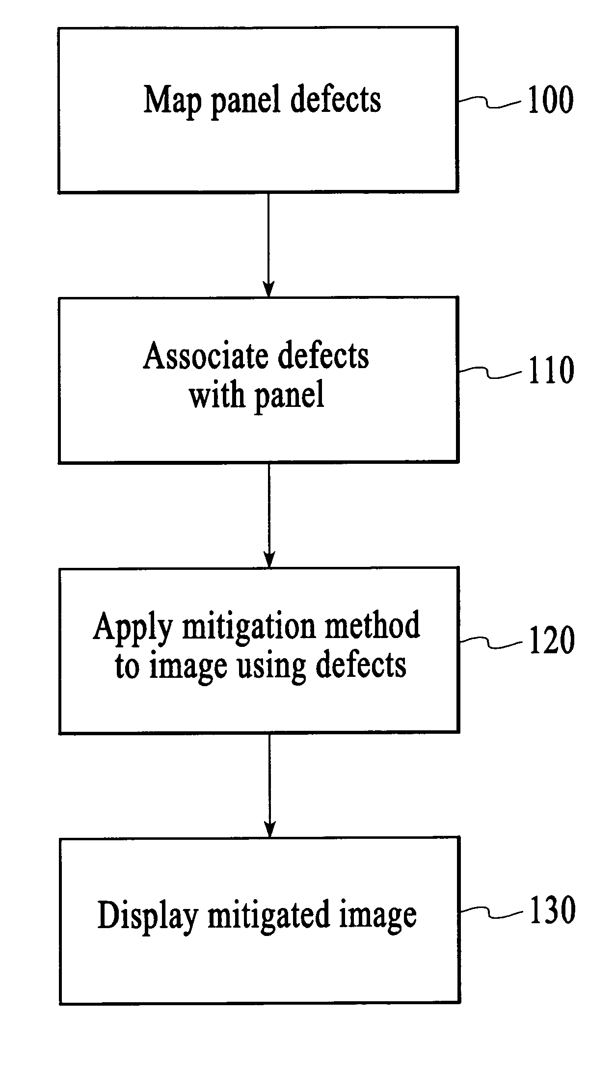
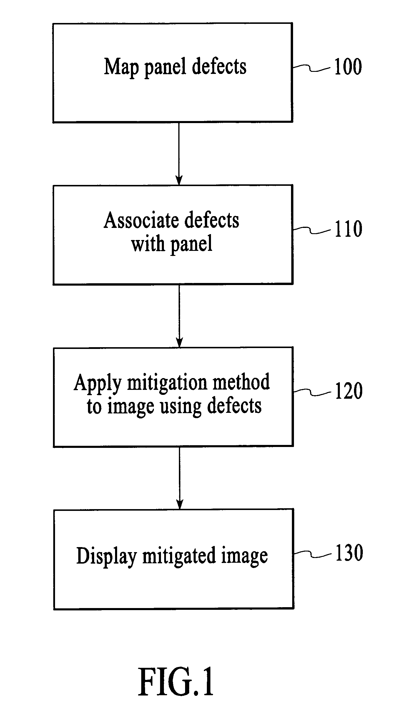
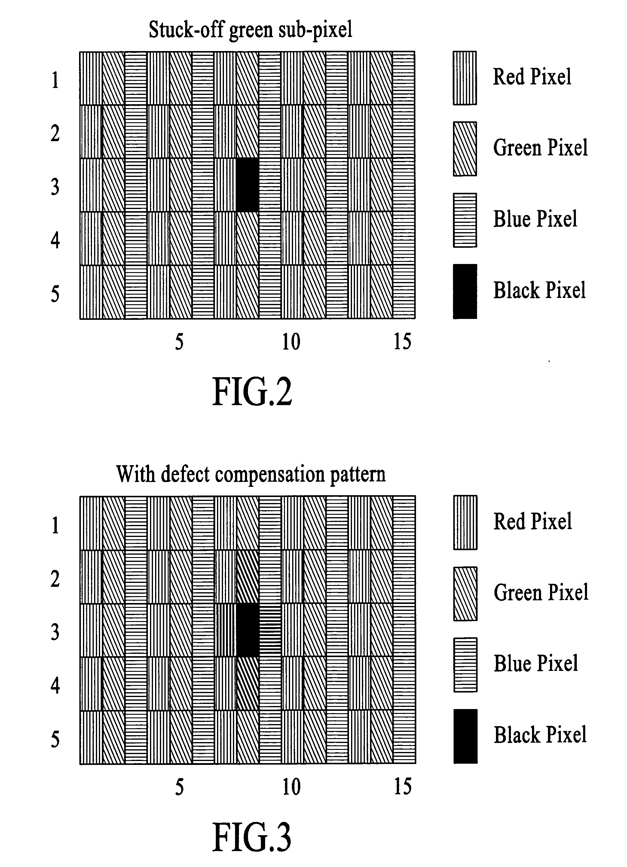
[0009] In accordance with the present invention, and as shown in the flowchart of FIG. 1, a display panel is first mapped 100 for defects. This mapping may be accomplished by completely automatic methods, as an example, by using test pattern generation coupled with image sensing to detect the presence or absence of pixels. The mapping may also be accomplished in a semi-automatic manner in which a human operator assists the defect mapping process. The result of the defect mapping is a data set identifying faulty pixels. Pixels are identified by location, and the nature of the fault, which at a minimum is stuck on or stuck off. Optionally, information such as pixel luminance may be recorded to identify defective pixels which turn partially on or off. With color panels, such as RGB panels, the luminance and chromaticity of the panel's primary colors are recorded for use in the defect correction models.

[0010] The accumulated data set identifying faulty pixels in a panel is associated 1...


PUM


Abstract

Defect mitigation in display panels. Defects in a display panel are mapped, and the defect information is associated with the display system or associated with the panel. During panel operation, the values of pixels neighboring defective pixels are altered to minimize their visibility to the observer. In a first model, luminance error caused by a defect is compensated by adjust neighboring pixels. In a second model, Error in luminance and one of the two chrominance channels is compensated by adjusting neighboring pixels. The defect mitigation methods seek to shift the errors introduced by defective pixels into high spatial frequency elements and chromatic elements, which the human eye is not sensitive to.

Description

TECHNICAL FIELD [0001] Embodiments in accordance with the invention are related to display panels, and more specifically, to defect mitigation in display panels. BACKGROUND [0002] Flat panel displays are quickly becoming a dominant display technology. They range from liquid crystal (LCD) RGB displays, to plasma displays, to light emitting diode (LED) and organic light emitting diode (OLED) displays, projection displays using single or multiple LCD elements, and single or multiple micro-mirror elements. [0003] A common problem shared by these technologies is yield. Perfect panels are very difficult to produce, and are very expensive. Pixel defects in LCD panels include stuck-on and stuck-off pixels. Typically, some number of defective pixels are allowed on a display panel. An ISO standard for pixel defects, ISO 13406-2, identifies three classes of standards for measuring pixel defects in flat panel displays. The most lenient class still only permits five full-brightness pixels, 15 fu...

Claims


Application Information

Patent Timeline
IPC IPC(8): G01R31/00
CPCG02F1/1309G09G2330/10G09G3/20H04N25/67
Inventor ZHANG, XUEMEIXIAO, FENG
Owner WISTRON CORP
Why Eureka
Try Eureka